
资料下载


零电压开关降压变换器提供最大功率密度、效率
分享资料个
零电压开关降压变换器提供最大功率密度、效率
与传统的脉冲宽度调制(PWM)或硬开关结构相比,使用谐振拓扑的降压变换器比基于传统结构的电源提供更高的性能。虽然晚了传统高密度、硬开关稳压器具有演化的改进的半导体集成、低电阻MOSFET,和先进的包装,他们的设计是不足以满足新的电力需求,主要是由于在调节MOSFET的开关损耗,提高开关频率或增加输入电压。
此外,传统的降压稳压器表现出更高的栅极驱动损耗,由于米勒电荷消耗在栅极驱动电路。同样,高侧MOSFET的体二极管传导有助于更高的功率损耗,由于反向恢复和长导(图1)。因此,必须克服或大幅降低这些损失,以实现调节器性能的任何显著提高。此外,硬开关拓扑需要一个比较大的输出电感,这增加了调节器的尺寸和成本。
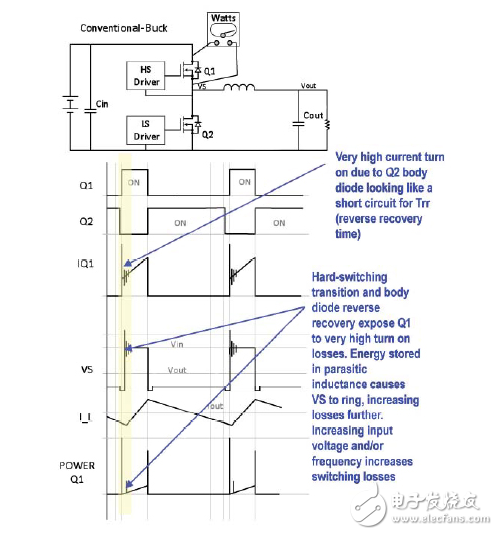
Figure 1: In conventional buck regulators, the hard-switching transition and body diode reverse recovery expose the high-side MOSFET Q1 to very high turn-on losses.
Benefits of zero-voltage switching
Another, better alternative is to use resonant topology like zero-voltage switching (ZVS), which enables operation at higher frequency and higher voltages without sacrificing efficiency and size. The ZVS-based regulators are also known as soft-switching regulators. Some key benefits of ZVS buck regulator topology include low turn-on losses, negligible body diode conduction time due to ideal rectifier switching, high-frequency operation maintained at high input voltage, simple internal compensation – which allows for high bandwidth, gain, and phase margin – and fast transient response with a small amount of output capacitance. What is more, it offers 20 ns minimum on time to support very high conversion ratios and delivers excellent light-load efficiency due to a high-efficiency biasing system combined with pulse skipping.
声明:本文内容及配图由入驻作者撰写或者入驻合作网站授权转载。文章观点仅代表作者本人,不代表电子发烧友网立场。文章及其配图仅供工程师学习之用,如有内容侵权或者其他违规问题,请联系本站处理。 举报投诉
- 相关下载
- 相关文章


