资料下载

adf7021高性能窄带收发器芯片数据表
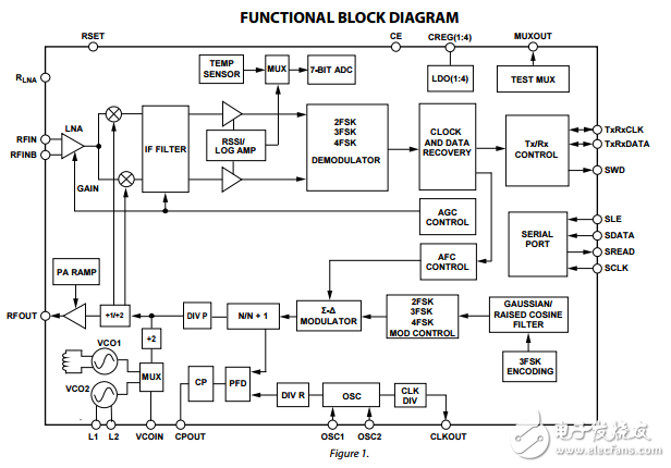
The ADF7021 is a high performance, low power, highly integrated 2FSK/3FSK/4FSK transceiver. It is designed to operate in the narrowband, license-free ISM bands, and in the licensed bands with frequency ranges of 80 MHz to 650 MHz and 862 MHz to 950 MHz. The device has both Gaussian and raised cosine transmit data filtering options to improve spectral efficiency for narrowband applications. It is suitable for circuit applications targeted at European ETSI EN 300 220, the Japanese ARIB STD-T67, the Chinese short range device regulations, and the North American FCC Part 15, Part 90, and Part 95 regulatory standards. A complete transceiver can be built using a small number of external discrete components, making the ADF7021 very suitable for price sensitive and area sensitive applications. The range of on-chip FSK modulation and data filtering options allows users greater flexibility in their choice of modulation schemes while meeting tight spectral efficiency requirements. The ADF7021 also supports protocols that dynamically switch between 2FSK/3FSK/4FSK to maximize communication range and data throughput. The transmit section contains dual voltage controlled oscillators (VCOs) and a low noise fractional-N PLL with an output resolution of 《1 ppm. The ADF7021 has a VCO using an internal LC tank (431 MHz to 475 MHz, 862 MHz to 950 MHz) and a VCO using an external inductor as part of its tank circuit (80 MHz to 650 MHz)。 The dual VCO design allows dual-band operation where the user can transmit and/or receive at any frequency supported by the internal inductor VCO and can also transmit and/or receive at a particular frequency band supported by the external inductor VCO. The frequency agile PLL allows the ADF7021 to be used in frequency hopping spread spectrum (FHSS) systems. Both VCOs operate at twice the fundamental frequency to reduce spurious emissions and frequency pulling problems. The transmitter output power is programmable in 63 steps from −16 dBm to +13 dBm, and has an automatic power ramp control to prevent spectral splatter and help meet regulatory standards. The transceiver RF frequency and modulation are programmable using a simple 3-wire interface. The device operates with a power supply range of 2.3 V to 3.6 V and can be powered down when not in use. A low IF architecture is used in the receiver (100 kHz), which minimizes power consumption and the external component count, yet avoids dc offset and flicker noise at low frequencies. The IF filter has programmable bandwidths of 12.5 kHz, 18.75 kHz, and 25 kHz. The ADF7021 supports a wide variety of programmable features including Rx linearity, sensitivity, and IF bandwidth, allowing the user to trade off receiver sensitivity and selectivity against current consumption, depending on the application. The receiver also features a patent-pending automatic frequency control (AFC) loop with programmable pull-in range that allows the PLL to track out the frequency error in the incoming signal. The receiver achieves an image rejection performance of 56 dB using a patent-pending IR calibration scheme that does not require the use of an external RF source. An on-chip ADC provides readback of the integrated temperature sensor, external analog input, battery voltage, and RSSI signal, which provides savings on an ADC in some applications. The temperature sensor is accurate to ±10°C over the full operating temperature range of −40°C to +85°C. This accuracy can be improved by performing a 1-point calibration at room temperature and storing the result in memory

声明:本文内容及配图由入驻作者撰写或者入驻合作网站授权转载。文章观点仅代表作者本人,不代表电子发烧友网立场。文章及其配图仅供工程师学习之用,如有内容侵权或者其他违规问题,请联系本站处理。 举报投诉
- 相关下载
- 相关文章


