
资料下载


8通道12位ADC/DAC芯片上可参考的SPI接口ad5592r数据表
分享资料个
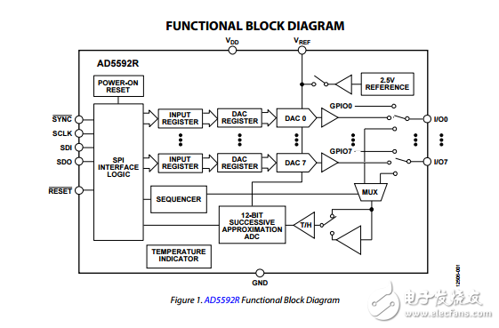
The AD5592R/AD5592R-1 have eight I/Ox pins (I/O0 to I/O7) that can be independently configured as digital-to-analog converter (DAC) outputs, analog-to-digital converter (ADC) inputs, digital outputs, or digital inputs. When an I/Ox pin is configured as an analog output, it is driven by a 12-bit DAC. The output range of the DAC is 0 V to VREF or 0 V to 2 × VREF. When an I/Ox pin is configured as an analog input, it is connected to a 12-bit ADC via an analog multiplexer. The input range of the ADC is 0 V to VREF or 0 V to 2 × VREF. The ADC has a total throughput rate of 400 kSPS. The I/Ox pins can also be configured as digital, general-purpose input or output (GPIO) pins. The state of the GPIO pins can be set or read back by accessing the GPIO write data register or the GPIO read configuration register, respectively, via a serial peripheral interface (SPI) write or read operation. The AD5592R/AD5592R-1 have an integrated 2.5 V, 25 ppm/°C reference, which is turned off by default, and an integrated temperature indicator, which gives an indication of the die temperature. The temperature value is read back as part of an ADC read sequence. The AD5592R/AD5592R-1 are available in 16-ball, 2 mm × 2 mm WLCSP, 16-lead, 3 mm × 3 mm LFCSP, and 16-lead TSSOP. The AD5592R/AD5592R-1 operate over a temperature range of −40°C to +105°C.

声明:本文内容及配图由入驻作者撰写或者入驻合作网站授权转载。文章观点仅代表作者本人,不代表电子发烧友网立场。文章及其配图仅供工程师学习之用,如有内容侵权或者其他违规问题,请联系本站处理。 举报投诉
- 相关下载
- 相关文章


