
资料下载


LC2 MOS 16位电压输出数模转换器AD7846数据表
分享资料个
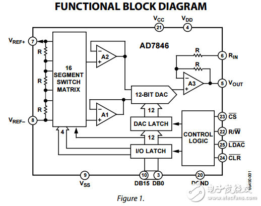
The AD7846 is a 16-bit DAC constructed with the Analog Devices, Inc., LC2 MOS process. It has VREF+ and VREF− reference inputs and an on-chip output amplifier. These can be configured to give a unipolar output range (0 V to +5 V, 0 V to +10 V) or bipolar output ranges (±5 V, ±10 V)。 The DAC uses a segmented architecture. The four MSBs in the DAC latch select one of the segments in a 16-resistor string. Both taps of the segment are buffered by amplifiers and fed to a 12-bit DAC, which provides a further 12 bits of resolution. This architecture ensures 16-bit monotonicity. Excellent integral linearity results from tight matching between the input offset voltages of the two buffer amplifiers. In addition to the excellent accuracy specifications, the AD7846 also offers a comprehensive microprocessor interface. There are 16 data I/O pins, plus control lines (CS, R/W, LDAC and CLR)。 R/W and CS allow writing to and reading from the I/O latch. This is the readback function, which is useful in ATE applications. LDAC allows simultaneous updating of DACs in a multi-DAC system and the CLR line will reset the contents of the DAC latch to 00…000 or 10…000 depending on the state of R/W.

声明:本文内容及配图由入驻作者撰写或者入驻合作网站授权转载。文章观点仅代表作者本人,不代表电子发烧友网立场。文章及其配图仅供工程师学习之用,如有内容侵权或者其他违规问题,请联系本站处理。 举报投诉
- 相关下载
- 相关文章


