资料下载

电磁兼容设计资料下载
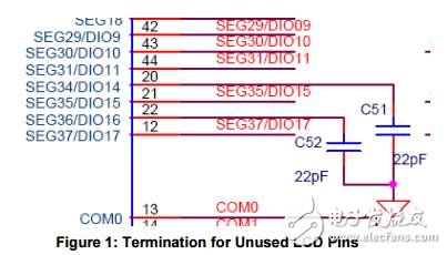
These pins cannot be configured and are dedicated LCD driver pins. In some designs, restrictions on the choice for LCD_NUM may require that some DIO/SEG pins are configured as LCD pins. If not connected to an LCD pin, these unused SEG pins should be terminated to DGND with 22 pF capacitors as shown in Figure 1.

If no LCD is used in the design, the pure segment pins can also be tied to DGND. LCD_E must be set to zero (power-up default), otherwise current will be drawn from the pins.
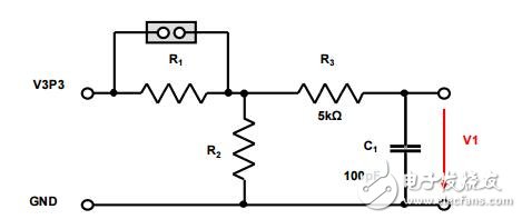
The V1 input pin detects power faults and provides a means to disable the hardware watchdog timer for debugging purposes. When the voltage at the V1 pin falls below +1.6 VDC (VBIAS), the device enters its power-down mode (brownout mode)。 The firmware decides whether to proceed from there to LCD or sleep mode or whether the IC stays in brownout mode. Since the hardware watchdog timer (WDT) is automatically disabled when the ICE_E pin is pulled high, the V1 pin need not have a jumper to V3P3 to disable the WDT for emulator connection.

声明:本文内容及配图由入驻作者撰写或者入驻合作网站授权转载。文章观点仅代表作者本人,不代表电子发烧友网立场。文章及其配图仅供工程师学习之用,如有内容侵权或者其他违规问题,请联系本站处理。 举报投诉
- 相关下载
- 相关文章


