
资料下载


NXP微控制器的BGA封装的PCB布线指南
分享资料个
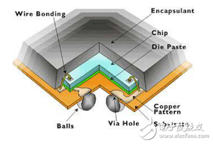
When building a BGA footprint the number one consideration is ensuring the ball pattern
and outline matches the device package. This includes correct orientation of ball A1,
matching all ball column x row locations, and the ball-to-ball pitch. Solder joint reliability is
also of primary concern. For cost sensitive applications, minimizing the number of PCB
layers required to route the BGA is a consideration. The BGA land pattern footprint plays
a key role in solder joint reliability, and the number of PCB layers required to route the
balls.
Land pad design
The PCB BGA land pads have to be designed to ensure solder joint reliability and
provide optimum manufacturability. The two basic types of BGA land pad design are:
• The Solder Mask Defined (SMD) land pad
• The Non-Solder Mask Defined (NSMD) land pad; recommended type for PC
Solder Mask Defined (SMD) land pad
The SMD type of BGA land pad design is characterized by the copper pad being larger
than the solder mask opening above this pad. Thus the solder joint area of the land pad
is defined by the opening in the solder mask.
声明:本文内容及配图由入驻作者撰写或者入驻合作网站授权转载。文章观点仅代表作者本人,不代表电子发烧友网立场。文章及其配图仅供工程师学习之用,如有内容侵权或者其他违规问题,请联系本站处理。 举报投诉
- 相关下载
- 相关文章


