
资料下载


32通道16/14位串行输入电压输出数模转换器ad5372/ad5373数据表
分享资料个
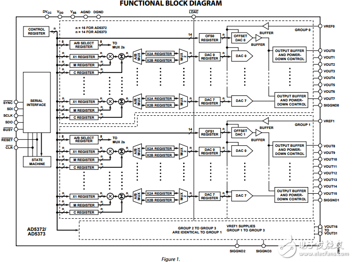
The AD5372/AD5373 contain 32 16-/14-bit DACs in 64-lead LQFP and LFCSP packages. The devices provide buffered voltage outputs with a nominal span of 4× the reference voltage. The gain and offset of each DAC can be independently trimmed to remove errors. For even greater flexibility, the device is divided into four groups of eight DACs. Two offset DACs allow the output range of the groups to be altered. Group 0 can be adjusted by Offset DAC 0, and Group 1 to Group 3 can be adjusted by Offset DAC 1. The AD5372/AD5373 offer guaranteed operation over a wide supply range: VSS from −16.5 V to −4.5 V and VDD from 9 V to 16.5 V. The output amplifier headroom requirement is 1.4 V operating with a load current of 1 mA. The AD5372/AD5373 have a high speed serial interface that is compatible with SPI, QSPI™, MICROWIRE™, and DSP interface standards and can handle clock speeds of up to 50 MHz. The DAC registers are updated on reception of new data. All the outputs can be updated simultaneously by taking the LDAC input low. Each channel has a programmable gain and an offset adjust register. Each DAC output is gained and buffered on chip with respect to an external SIGGNDx input. The DAC outputs can also be switched to SIGGNDx via the CLR pin.
声明:本文内容及配图由入驻作者撰写或者入驻合作网站授权转载。文章观点仅代表作者本人,不代表电子发烧友网立场。文章及其配图仅供工程师学习之用,如有内容侵权或者其他违规问题,请联系本站处理。 举报投诉
- 相关下载
- 相关文章


