
资料下载


LC2 MOS四路8位数模转换器单独的基准输入AD7225数据表
分享资料个
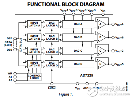
The AD7225 contains four 8-bit voltage output digital-toanalog converters, with output buffer amplifiers and interface logic on a single monolithic chip. Each DAC has a separate reference input terminal. No external trims are required to achieve full specified performance for the part. The double-buffered interface logic consists of two 8-bit registers per channel—an input register and a DAC register. Control Input A0 and Control Input A1 determine which input register is loaded when WR goes low. Only the data held in the DAC registers determines the analog outputs of the converters. The double-buffering allows simultaneous update of all four outputs under control of LDAC. All logic inputs are TTL and CMOS (5 V) level compatible, and the control logic is speed compatible with most 8-bit microprocessors. Specified performance is guaranteed for input reference voltages from 2 V to 12.5 V when using dual supplies. The part is also specified for single-supply operation using a reference of 10 V. Each output buffer amplifier is capable of developing 10 V across a 2 kΩ load. The AD7225 is fabricated on an all ion-implanted, high speed, linear-compatible CMOS (LC2 MOS) process, which is specifically developed to integrate high speed digital logic circuits and precision analog circuitry on the same chip.

声明:本文内容及配图由入驻作者撰写或者入驻合作网站授权转载。文章观点仅代表作者本人,不代表电子发烧友网立场。文章及其配图仅供工程师学习之用,如有内容侵权或者其他违规问题,请联系本站处理。 举报投诉
- 相关下载
- 相关文章


