资料下载

14位MSPS的160个DAC的插值滤波器AD9772A数据表
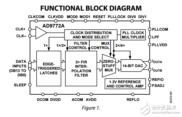
The AD9772A is a single-supply, oversampling, 14-bit digitalto-analog converter (DAC) optimized for baseband or IF waveform reconstruction applications requiring exceptional dynamic range. Manufactured on an advanced CMOS process, it integrates a complete, low distortion 14-bit DAC with a 2× digital interpolation filter and clock multiplier. The on-chip PLL clock multiplier provides all the necessary clocks for the digital filter and the 14-bit DAC. A flexible differential clock input allows for a single-ended or differential clock driver for optimum jitter performance. For baseband applications, the 2× digital interpolation filter provides a low-pass response, thus providing as much as a threefold reduction in the complexity of the analog reconstruction filter. It does so by multiplying the input data rate by a factor of 2 while suppressing the original upper in-band image by more than 73 dB. For direct IF applications, the 2× digital interpolation filter response can be reconfigured to select the upper in-band image (that is, the high-pass response) while suppressing the original baseband image. To increase the signal level of the higher IF images and their pass-band flatness in direct IF applications, the AD9772A also features a zero-stuffing option in which the data following the 2× interpolation filter is upsampled by a factor of 2 by inserting midscale data samples. The AD9772A can reconstruct full-scale waveforms with bandwidths of up to 67.5 MHz while operating at an input data rate of 160 MSPS. The 14-bit DAC provides differential current outputs to support differential or single-ended applications. A segmented current source architecture is combined with a proprietary switching technique to reduce spurious components and enhance dynamic performance. Matching between the two current outputs ensures enhanced dynamic performance in a differential output configuration. The differential current outputs can be fed into a transformer or a differential op amp topology to obtain a single-ended output voltage using an appropriate resistive load.

声明:本文内容及配图由入驻作者撰写或者入驻合作网站授权转载。文章观点仅代表作者本人,不代表电子发烧友网立场。文章及其配图仅供工程师学习之用,如有内容侵权或者其他违规问题,请联系本站处理。 举报投诉
- 相关下载
- 相关文章


