
资料下载


EE241 Advanced Digital Integrated Circuits Lecture17
分享资料个
z Supply current is brought on
chip at specific locations
» on the edge for most chips
which are peripherally
bonded
» distributed over the area of
the chip for area bonded (C4,
solder ball) chips
z Loads consume this current at
different locations on the chip
at different times
z There is often a large parasitic
inductance associated with
each bond-wire or solder-ball
(0.1-10nH)
z Current is distributed from
the bond pads to the loads
on thin metal wires
» 0.04Ω/ typical
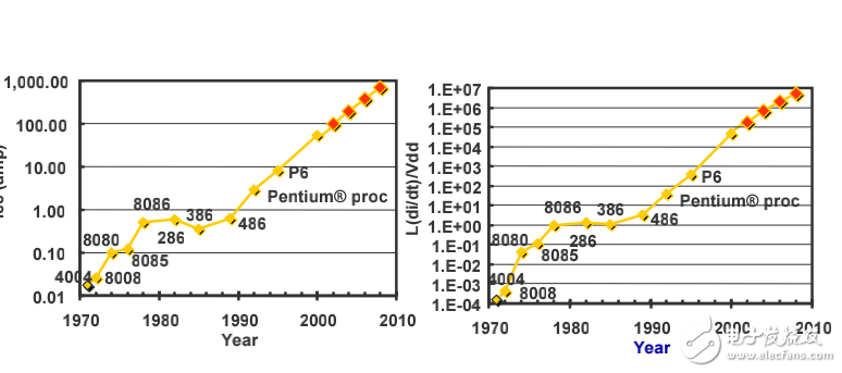
z Load currents may be very
high
» average current may be as
large as 20A for very hot
chips (50W at 2.5V)
» peak current may be 4-5x
this amount (100A!)
z L di/dt of bond wire and IR
drop across on-chip wires
are often a major source of
supply noise
声明:本文内容及配图由入驻作者撰写或者入驻合作网站授权转载。文章观点仅代表作者本人,不代表电子发烧友网立场。文章及其配图仅供工程师学习之用,如有内容侵权或者其他违规问题,请联系本站处理。 举报投诉
- 相关下载
- 相关文章


