
资料下载


ADP1828同步降压PWM降压DC-DC控制器数据表
分享资料个
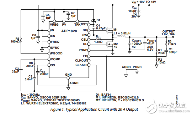
The ADP1828 is a versatile and synchronous PWM voltage mode buck controller. It drives an all N-channel power stage to regulate an output voltage as low as 0.6 V to 85% of the input voltage and is sized to handle large MOSFETs for point-of-load regulators. The ADP1828 is ideal for a wide range of high power applications, such as DSP and processor core I/O power, and general-purpose power in telecommunications, medical imaging, PC, gaming, and industrial applications. It operates from input bias voltages of 3 V to 20 V with an internal LDO that generates a 5 V output for input bias voltages greater than 5.5 V. The ADP1828 operates at a pin-selectable, fixed switching frequency of either 300 kHz or 600 kHz, or at any frequency between 300 kHz and 600 kHz with a resistor. The switching frequency can also be synchronized to an external clock up to 2× the part’s nominal oscillator frequency. The clock output can be used for synchronizing additional ADP1828s (or the ADP1829 controllers), thus eliminating the need for an external clock source. The ADP1828 includes soft start protection to limit any inrush current from the input supply during startup, reverse current protection during soft start for a precharged output, as well as a unique adjustable lossless current-limit scheme utilizing external MOSFET RDSON sensing. For applications requiring power-supply sequencing, the ADP1828 provides a tracking input that allows the output voltage to track during startup, shutdown, and faults. The additional supervisory and control features include thermal overload, undervoltage lockout, and power good. The ADP1828 operates over the −40°C to +125°C junction temperature range and is available in a 20-lead QSOP and 20- lead, 4mm × 4mm LFCSP.

声明:本文内容及配图由入驻作者撰写或者入驻合作网站授权转载。文章观点仅代表作者本人,不代表电子发烧友网立场。文章及其配图仅供工程师学习之用,如有内容侵权或者其他违规问题,请联系本站处理。 举报投诉
- 相关下载
- 相关文章


