资料下载

ADP5065快速充电电池电源管理器路径和USB兼容性
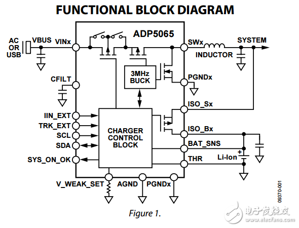
The ADP5065 charger is fully compliant with the USB 2.0, USB 3.0, and USB Battery Charging Specification 1.1 and enables charging via the mini USB VBUS pin from a wall charger, car charger, or USB host port. The ADP5065 operates from a 4 V to 5.5 V input voltage range but is tolerant of voltages of up to 20 V. This alleviates the concerns about the USB bus spiking during disconnect or connect scenarios. The ADP5065 also features an internal FET between the dc-todc charger output and the battery. This permits battery isolation and, hence, system powering under a dead battery or no battery scenario, which allows for immediate system function on connection to a USB power supply. Based on the type of USB source, which is detected by an external USB detection chip, the ADP5065 can be set to apply the correct current limit for optimal charging and USB compliance. The ADP5065 comes in a very small and low profile 20-lead WLCSP (0.5 mm pitch spacing) package. The overall solution requires only five small, low profile external components consisting of four ceramic capacitors (one of which is the battery filter capacitor), one multilayer inductor. In addition to these components, there is one optional dead battery situation default setting resistor. This configuration enables a very small PCB area to provide an integrated and performance enhancing solution to USB battery charging and power rail provision.

声明:本文内容及配图由入驻作者撰写或者入驻合作网站授权转载。文章观点仅代表作者本人,不代表电子发烧友网立场。文章及其配图仅供工程师学习之用,如有内容侵权或者其他违规问题,请联系本站处理。 举报投诉
- 相关下载
- 相关文章


