
资料下载


建设高降压比降压转换器的许多选择
分享资料个
建设高降压比降压转换器的许多选择
设计高降压比DC / DC电源转换器的转换是不平凡的,特别是当from 48 VDC输出和输入到3.3伏以下,因为高密度的效率和最小的维护成本是个挑战。这样的DC / DC电源转换器are primarily needed in通信系统和数据中心populated with computers with现代DSP板,FPGA,ASIC voltages and ranging from 3.3 V和要求较低。to avoid大厦高降压比Buck变换器中,利用总线转换器designers have been to further down the步流行的总线电压48 VDC in such Systems to level of中间电压12 V或24 V,低。adding that is to another降压阶段,从而简化分布式电源架构的设计。This has been adding to the cost and Space of the system while also reducing the overall板效率的性能。
多年来,为了消除中间功率转换阶段,一些制造商已经交付了这样的高阶比转换器的高效率和密度,以牺牲更高的成本。例如,Vicor结合其硅砌块如PRM和VTM模块产生一个孤立的DC / DC解决方案,以48伏直流母线电压并将其转换为低处理器的核心电压在1 V与英特尔的vr12.0和VR12.5本规。最近,Vicor扩大其导频控制泛音再现酷家庭的高密度,隔离直流/直流零电压开关(ZVS)变换器模块的新成员提供48 V输入和3.3 V输出在18的这样的一个例子是pi3101-00-hviz。
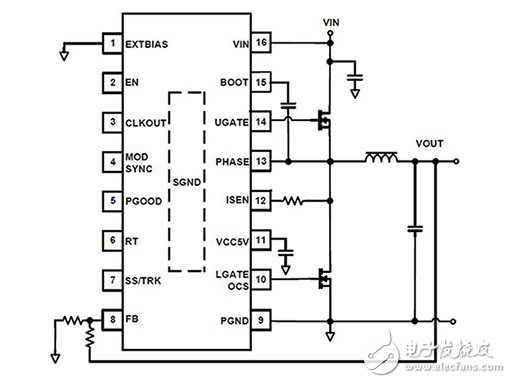
At the same time Efficient Power Conversion (EPC) has demonstrated a 48 V to 1.2 V non-isolated buck converter using its enhancement-mode gallium nitride (eGaN) FETs2. EPC’s initial demonstration incorporated first-generation 100 V eGaN FETs like EPC1001 and EPC1007 to enable a non-isolated buck converter capable of operating from 48 V input and generating low output of 1.2 V. The new-generation versions like EPC2001 and EPC2007 can offer further improvement in efficiency with higher reliability and cost competitiveness, according to the

声明:本文内容及配图由入驻作者撰写或者入驻合作网站授权转载。文章观点仅代表作者本人,不代表电子发烧友网立场。文章及其配图仅供工程师学习之用,如有内容侵权或者其他违规问题,请联系本站处理。 举报投诉
- 相关下载
- 相关文章


