
资料下载


AN-1645的LM4702芯片驱动MOSFET输出级
分享资料个
MOSFET Amplifier Design
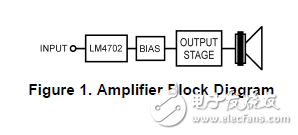
Figure 1 shows the basic block diagram of an amplifier using the LM4702. The amplifier consists of three building blocks, the LM4702, the bias stage, and the output stage (there are no protection circuits)。 Each stage will be covered in detail. The power supply design will not be covered as a basic unregulated supply consisting of a transformer, a bridge rectifier, with noise and reservoir capacitors is well known and common.
The LM4702 is a high voltage driver that includes the input stage and voltage amplifier stage (VAS) of a power amplifier. The LM4702, with feedback from the output stage, sets the gain and is externally compensated to set the slew rate. The outputs of the LM4702 drive the top and bottom sides of the bias and output stages. The LM4702 performance details are limited to basic recommendations on ranges for gain, slew rate, and the component types that achieve the best performance.
The bias stage performs two functions. First, it sets the DC bias voltage and resulting bias current in the output stage for Class A, AB or B operation. Second, it allows thermal compensation that maintains steady bias current as the output stage devices vary in temperature. As will be shown, certain devices do not need temperature compensation and the bias stage becomes as simple as a resistor. Other devices will need thermal tracking and temperature compensation controlled by the bias stage.
The output stage is a basic Source-Follower stage using a single pair of complementary N-channel and Pchannel transistors for simplicity. The same output stage design will be used for all devices listed in Table 1.

声明:本文内容及配图由入驻作者撰写或者入驻合作网站授权转载。文章观点仅代表作者本人,不代表电子发烧友网立场。文章及其配图仅供工程师学习之用,如有内容侵权或者其他违规问题,请联系本站处理。 举报投诉
- 相关下载
- 相关文章


