资料下载

半导体射频开关:小型但高性能电路元件
半导体射频开关:小型但高性能电路元件
RF开关用于从多个可用源中选择所需信号,或者将信号路由到所需信道,例如分集天线系统、雷达和测试和测量装置。开关(有时称为继电器)可以使用机电(EM)的设计类似于一个非射频开关,但这些现在已经被开关IC所取代,除了在高功率应用在集成电路的不足,以及一些非常特殊的情况下或在开关需要许多波兰人(联系人)。
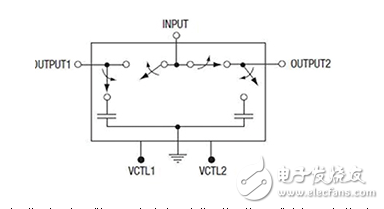
也有RF开关基于MEMS技术复制的机电设计,但使用IC制造技术。本文重点研究基于IC的固态开关,有一个单刀双掷开关开始(单刀双掷)排列(图1),并且通常与FET和PIN二极管为核心的开关元件的建立。

Figure 1: An SPDT RF switch is conceptually simple, with a control signal directing the switch to route the input to either one of two possible outputs. (Courtesy of Skyworks Solutions)
These are many parameters which define RF switch performance, and most must be characterized versus supply voltage, temperature, frequency, power level, and other factors. Some are especially critical in a given application, while others may not be as vital. Note that most RF switches are designed for 50 Ω operation, but some are designed for the 75 Ω standard of cable TV. Given the high frequencies at which these switches operate, many vendors now offer S-parameters and Smith charts as parts for their data sheet specifications (for background see the TechZone article “The Smith Chart: An ‘Ancient’ Graphical Tool Still Vital in RF Design”), to assist engineers in determining overall signal-path performance, matching component impedances for minimal loss, and modeling-system performance.
声明:本文内容及配图由入驻作者撰写或者入驻合作网站授权转载。文章观点仅代表作者本人,不代表电子发烧友网立场。文章及其配图仅供工程师学习之用,如有内容侵权或者其他违规问题,请联系本站处理。 举报投诉
- 相关下载
- 相关文章


