
资料下载


cy7c1061dv3316兆位(1M×16)静态RAM
分享资料个
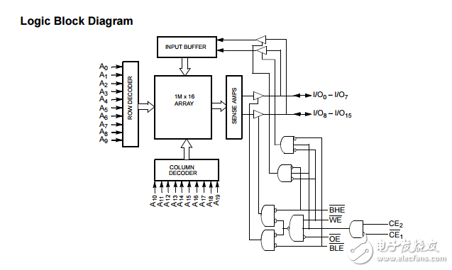
The CY7C1061DV33 is a high performance CMOS Static RAM organized as 1,048,576 words by 16 bits. To write to the device, take Chip Enables (CE1 LOW and CE2 HIGH) and Write Enable (WE) input LOW. If Byte Low Enable (BLE) is LOW, then data from I/O pins (I/O0 through I/O7), is written into the location specified on the address pins (A0 through A19)。 If Byte High Enable (BHE) is LOW, then data from I/O pins (I/O8 through I/O15) is written into the location specified on the address pins (A0 through A19)。 To read from the device, take Chip Enables (CE1 LOW and CE2 HIGH) and Output Enable (OE) LOW while forcing the Write Enable (WE) HIGH. If Byte Low Enable (BLE) is LOW, then data from the memory location specified by the address pins appears on I/O0 to I/O7. If Byte High Enable (BHE) is LOW, then data from memory appears on I/O8 to I/O15. See Truth Table on page 12 for a complete description of Read and Write modes. The input or output pins (I/O0 through I/O15) are placed in a high impedance state when the device is deselected (CE1 HIGH/CE2 LOW), the outputs are disabled (OE HIGH), the BHE and BLE are disabled (BHE, BLE HIGH), or during a write operation (CE1 LOW, CE2 HIGH, and WE LOW)。 The CY7C1061DV33 is available in a 54-pin TSOP II package with center power and ground (revolutionary) pinout, and 48-ball VFBGA packages. For a complete list of related documentation, click here.

声明:本文内容及配图由入驻作者撰写或者入驻合作网站授权转载。文章观点仅代表作者本人,不代表电子发烧友网立场。文章及其配图仅供工程师学习之用,如有内容侵权或者其他违规问题,请联系本站处理。 举报投诉
- 相关下载
- 相关文章


