
资料下载


LBCA2HNZYZ蓝牙低能耗模块Dialog半导体芯片数据表
分享资料个
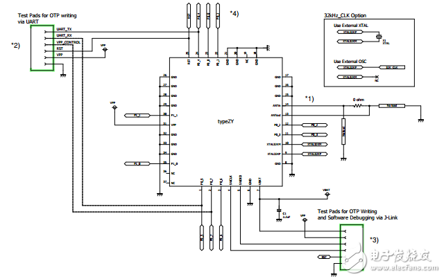
1) ANTout and ANTin are to be connected with pi-matching network. Connected line is recommended to be as short as possible. *2) Connection is necessary for writing program to the OTP via UART. Other GPIO pin can be used for VPP_CONTROL instead of P0_7. Please see the document “Hardware setup Guide for OTP Programming”。 Other pairs of GPIO can be used for UART instead of P0_4 and P0_5. Please see the document “Overview of DA1458X Initial Boot Sequence and Available Interface Pins”。 *3) Connection is necessary for software debugging in your product via J-Link. OTP writing can also be done using J-Link. Please see the document “Hardware Setup for Software Debugging”。 RST input logic should be inverted externally if J-Link reset is enabled. *4) 10 GPIOs (P0_0 to P0_7, P1_0 and P1_1) are available for multipurpose use. P0_0 to P0_3 can be used for analog input. Note: XTAL32K_DISABLE_AMPREG register should be ‘1’ for using external OSC. See DA14580 datasheet for more details. Note: Internal RCX oscillator might be functional for sleep clock instead of external 32kHz XTAL / OSC under some limitations noted below: - Environment temperature change is flat, connection interval 《 2sec. - Confirmation in actual condition should be done enough by the customer’s responsibility.

声明:本文内容及配图由入驻作者撰写或者入驻合作网站授权转载。文章观点仅代表作者本人,不代表电子发烧友网立场。文章及其配图仅供工程师学习之用,如有内容侵权或者其他违规问题,请联系本站处理。 举报投诉
- 相关下载
- 相关文章


