
资料下载


2.7V至5.25V微功耗双通道125KSPS,8引脚12位模数转换器AD7887数据表
分享资料个
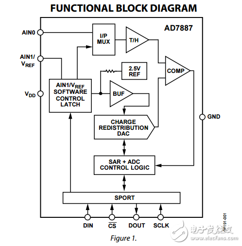
The AD7887 is a high speed, low power, 12-bit analog-to-digital converter (ADC) that operates from a single 2.7 V to 5.25 V power supply. The AD7887 is capable of 125 kSPS throughput rate. The input track-and-hold acquires a signal in 500 ns and features a single-ended sampling scheme. The output coding for the AD7887 is straight binary, and the part is capable of converting full power signals of up to 2.5 MHz. The AD7887 can be configured for either dual- or single-channel operation via the on-chip control register. There is a default single-channel mode that allows the AD7887 to be operated as a read-only ADC. In single-channel operation, there is one analog input (AIN0) and the AIN1/VREF pin assumes its VREF function. This VREF pin allows the user access to the part’s internal 2.5 V reference, or the VREF pin can be overdriven by an external reference to provide the reference voltage for the part. This external reference voltage has a range of 2.5 V to VDD. The analog input range on AIN0 is 0 to VREF. In dual-channel operation, the AIN1/VREF pin assumes its AIN1 function, providing a second analog input channel. In this case, the reference voltage for the part is provided via the VDD pin. As a result, the input voltage range on both the AIN0 and AIN1 inputs is 0 to VDD. CMOS construction ensures low power dissipation of typically 2 mW for normal operation and 3 μW in power-down mode. The part is available in an 8-lead, 0.15-inch-wide narrow body SOIC and an 8-lead MSOP package.

声明:本文内容及配图由入驻作者撰写或者入驻合作网站授权转载。文章观点仅代表作者本人,不代表电子发烧友网立场。文章及其配图仅供工程师学习之用,如有内容侵权或者其他违规问题,请联系本站处理。 举报投诉
- 相关下载
- 相关文章


