
资料下载


20毫瓦功率2.3 V至5.5 V 75兆赫完全DDS的AD9834数据表
分享资料个
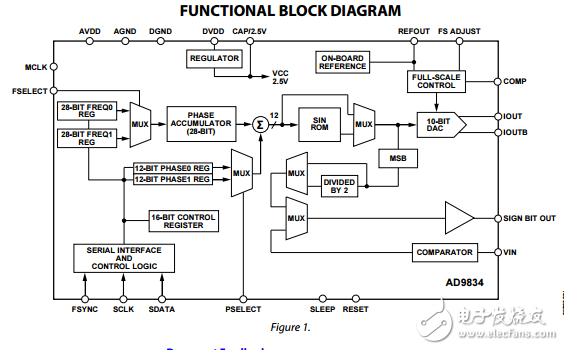
The AD9834 is a 75 MHz low power DDS device capable of producing high performance sine and triangular outputs. It also has an on-board comparator that allows a square wave to be produced for clock generation. Consuming only 20 mW of power at 3 V makes the AD9834 an ideal candidate for power-sensitive applications.
Capability for phase modulation and frequency modulation is provided. The frequency registers are 28 bits; with a 75 MHz clock rate, resolution of 0.28 Hz can be achieved. Similarly, with a 1 MHz clock rate, the AD9834 can be tuned to 0.004 Hz resolution. Frequency and phase modulation are affected by loading registers through the serial interface and toggling the registers using software or the FSELECT pin and PSELECT pin, respectively. The AD9834 is written to using a 3-wire serial interface. This serial interface operates at clock rates up to 40 MHz and is compatible with DSP and microcontroller standards. The device operates with a power supply from 2.3 V to 5.5 V. The analog and digital sections are independent and can be run from different power supplies, for example, AVDD can equal 5 V with DVDD equal to 3 V. The AD9834 has a power-down pin (SLEEP) that allows external control of the power-down mode. Sections of the device that are not being used can be powered down to minimize the current consumption. For example, the DAC can be powered down when a clock output is being generated. The part is available in a 20-lead TSSOP

声明:本文内容及配图由入驻作者撰写或者入驻合作网站授权转载。文章观点仅代表作者本人,不代表电子发烧友网立场。文章及其配图仅供工程师学习之用,如有内容侵权或者其他违规问题,请联系本站处理。 举报投诉
- 相关下载
- 相关文章


