
资料下载


3.3v 32K×8的CMOS SRAM(常见的I/O)AS7C3256A
分享资料个
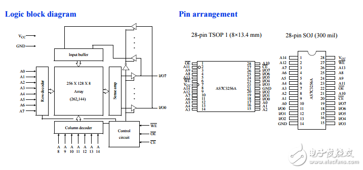
The AS7C3256A is a 3.3V high-performance CMOS 262,144-bit Static Random-Access Memory (SRAM) device organized as 32,768 words × 8 bits. It is designed for memory applications requiring fast data access at low voltage, including PentiumTM, PowerPCTM, and portable computing. Alliance’s advanced circuit design and process techniques permit 3.3V operation without sacrificing performance or operating margins. The device enters standby mode when CE is high. CMOS standby mode consumes 7.2 mW. Normal operation offers 75% power reduction after initial access, resulting in significant power savings during CPU idle, suspend, and stretch mode. Equal address access and cycle times (tAA, tRC, tWC) of 10/12/15/20 ns with output enable access times (tOE) of 5, 6, 7, 8 ns are ideal for high-performance applications. The chip enable (CE) input permits easy memory expansion with multiple-bank memory organizations. A write cycle is accomplished by asserting chip enable (CE) and write enable (WE) LOW. Data on the input pins I/O0-I/O7 is written on the rising edge of WE (write cycle 1) or CE (write cycle 2)。 To avoid bus contention, external devices should drive I/O pins only after outputs have been disabled with output enable (OE) or write enable (WE)。 A read cycle is accomplished by asserting chip enable (CE) and output enable (OE) LOW, with write enable (WE) high. The chip drives I/O pins with the data word referenced by the input address. When chip enable or output enable is high, or write enable is low, output drivers stay in high-impedance mode. All chip inputs and outputs are TTL-compatible. Operation is from a single 3.3 ±0.3V supply. The AS7C3256A is packaged in high volume industry standard packages.

声明:本文内容及配图由入驻作者撰写或者入驻合作网站授权转载。文章观点仅代表作者本人,不代表电子发烧友网立场。文章及其配图仅供工程师学习之用,如有内容侵权或者其他违规问题,请联系本站处理。 举报投诉
- 相关下载
- 相关文章


