
资料下载


低压CMOS输出低抖动时钟发生器ad9523-1数据表
分享资料个
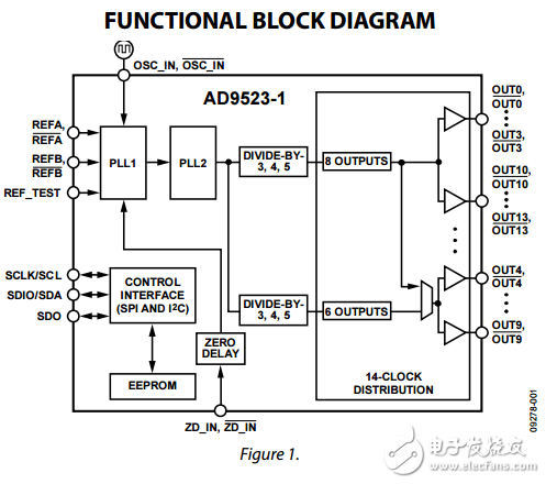
The AD9523-1 provides a low power, multi-output, clock distribution function with low jitter performance, along with an on-chip PLL and VCO with two VCO dividers. The on-chip VCO tunes from 2.94 GHz to 3.1 GHz. The AD9523-1 is designed to support the clock requirements for long term evolution (LTE) and multicarrier GSM base station designs. It relies on an external VCXO to provide the reference jitter cleanup to achieve the restrictive low phase noise requirements necessary for acceptable data converter SNR performance. The input receivers, oscillator, and zero delay receiver provide both single-ended and differential operation. When connected to a recovered system reference clock and a VCXO, the device generates 14 low noise outputs with a range of 1 MHz to 1 GHz, and one dedicated buffered output from the input PLL (PLL1)。 The frequency and phase of one clock output relative to another clock output can be varied by means of a divider phase select function that serves as a jitter-free, coarse timing adjustment in increments that are equal to half the period of the signal coming out of the VCO. An in-package EEPROM can be programmed through the serial interface to store user-defined register settings for power-up and chip reset.

声明:本文内容及配图由入驻作者撰写或者入驻合作网站授权转载。文章观点仅代表作者本人,不代表电子发烧友网立场。文章及其配图仅供工程师学习之用,如有内容侵权或者其他违规问题,请联系本站处理。 举报投诉
- 相关下载
- 相关文章


