
资料下载


低电压输出低抖动时钟发生器ad9525数据表
分享资料个
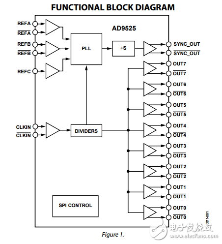
The AD9525 is designed to support converter clock requirements for long-term evolution (LTE) and multicarrier GSM base station designs. The AD9525 provides a low power, multioutput, clock distribution function with low jitter performance, along with an on-chip PLL that can be used with an external VCO or VCXO. The VCO input and eight LVPECL outputs can operate up to a frequency of 3.6 GHz. All outputs share a common divider that can provide a division of 1 to 6. The AD9525 offers a dedicated output that can be used to provide a programmable signal for resetting or synchronizing a data converter. The output signal is activated by a SPI write. The AD9525 is available in a 48-lead LFCSP and can be operated from a single 3.3 V supply. The external VCXO or VCO can have an operating voltage of up to 5.5 V. The AD9525 operates over the extended industrial temperature range of −40°C to +85°C.

声明:本文内容及配图由入驻作者撰写或者入驻合作网站授权转载。文章观点仅代表作者本人,不代表电子发烧友网立场。文章及其配图仅供工程师学习之用,如有内容侵权或者其他违规问题,请联系本站处理。 举报投诉
- 相关下载
- 相关文章


