
资料下载


系数RAM访问机制
汽车玩家
分享资料个
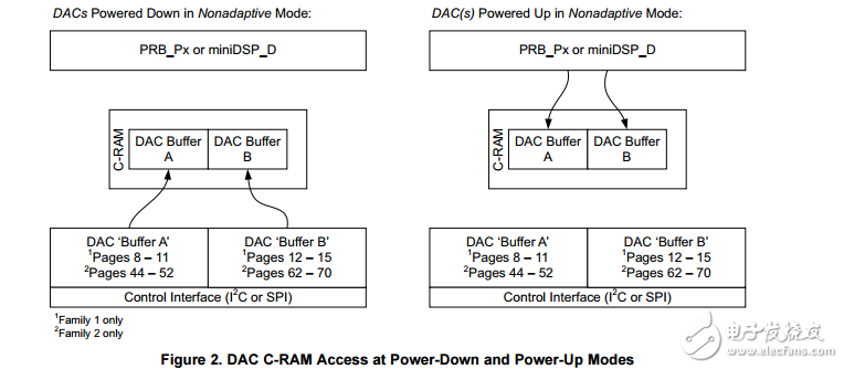
Introduction For clarity, this application report organizes several devices into two families that share a common coefficient RAM (C-RAM) access mechanism:
• Family 1: – TSC2117 – TLV320AIC3111 – TLV320AIC3100 – TLV320AIC3120 – TLV320DAC3120 – TLV320DAC3101 – TLV320DAC3100 – TLV320AIC36 – TLV320ADC3101 – TLV320ADC3001
• Family 2: – TLV320AIC3254 – TLV320AIC3204 – TLV320AIC3253 – TLV320AIC3256
Note that some features do not apply to some devices within a family. For instance, the TLV320ADC3101 does not have digital-to-analog converter (DAC) channels, therefore, any mention of DAC channel filtering does not apply for this device. In a similar fashion, the TLV320AIC3204 does not have a programmable miniDSP, therefore, any miniDSP mention does not apply for this device. Although the C-RAM access mechanism can be the same, some devices differ on the C-RAM size and word length. The following conventions are used throughout this document: • miniDSP_D – miniDSP associated with the DAC channel. • miniDSP_A – miniDSP associated with the analog-to-digital converter (ADC) channel. • PRB_Px – DAC processing block x, where x denotes any processing block for playback. • PRB_Ry – ADC processing block y, where y denotes any processing block for recording. • DAC(s) – it means that a statement applies if an action is performed to one or both DACs. • DACs – it means that a statement applies if an action is performed to both DACs. • ADC(s) – it means that a statement applies if an action is performed to one or both ADCs. • ADCs – it means that a statement applies if an action is performed to both ADCs. • Page X or Page Y – X refers to the first page of DAC Buffer A whereas Y refers to the first page of ADC Buffer A.
声明:本文内容及配图由入驻作者撰写或者入驻合作网站授权转载。文章观点仅代表作者本人,不代表电子发烧友网立场。文章及其配图仅供工程师学习之用,如有内容侵权或者其他违规问题,请联系本站处理。 举报投诉
- 相关下载
- 相关文章


