
资料下载


关于Basy3实验板详细的资料
gaohuiguo88
分享资料个
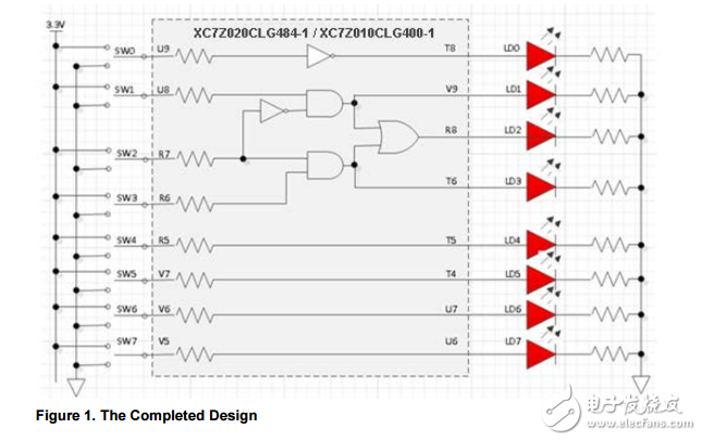
Introduction This lab guides you through the process of using Vivado IDE to create a simple HDL design targeting the Zynq device. You will simulate, synthesize, and implement the design with default settings. Finally, you will generate the bitstream and download it in to the hardware to verify the design functionality Objectives After completing this lab, you will be able to: • Create a Vivado project sourcing HDL model(s) and targeting a specific FPGA device located on the ZedBoard or Zybo • Use the provided Xilinx Design Constraint (XDC) file to constrain the pin locations • Simulate the design using the Vivado simulator • Synthesize and implement the design • Generate the bitstream • Configure the FPGA using the generated bitstream and verify the functionality Procedure This lab is broken into steps that consist of general overview statements providing information on the detailed instructions that follow. Follow these detailed instructions to progress through the lab1. Design Description The design consists of some inputs directly connected to the corresponding output LEDs. Other inputs are logically operated on before the results are output on the remaining LEDs as shown in Figure 1.
声明:本文内容及配图由入驻作者撰写或者入驻合作网站授权转载。文章观点仅代表作者本人,不代表电子发烧友网立场。文章及其配图仅供工程师学习之用,如有内容侵权或者其他违规问题,请联系本站处理。 举报投诉
-
 小婉紫
2019-04-22
0 回复 举报资料需要 收起回复
小婉紫
2019-04-22
0 回复 举报资料需要 收起回复
- 相关下载
- 相关文章


