资料下载

无光反激拓扑简化了隔离DCDC变换器的设计
无光反激拓扑简化了隔离DC/DC变换器的设计
除了被用在电信和数据通信系统中,直流输出也在许多其他噪声敏感的应用如汽车蓄电池的充电要求,中间总线电压为各种电子负载,和工业品。虽然反激拓扑是流行的隔离DC / DC转换器应用,由于它相对简单和成本较低的替代孤立的拓扑结构,设计传统的反激式是不容易的,因为变压器需要精心设计,环补偿可以是复杂的。此外,它需要一个光耦或额外的变压器绕组反馈输出电压从二次侧,以维持输出精度。
光耦合器的传输延迟、老化和增益变化使复环补偿和反激变换器的稳定性复杂化,同时限制了变换器的瞬态响应。此外,光耦合器消耗功率,增加电源的成本和物理尺寸。设计一个高性能变压器与额外的绕组可以采取大量的时间,因为有一个有限的选择现成的变压器。最后,使用一个额外的绕组增加了变压器的物理尺寸和成本。

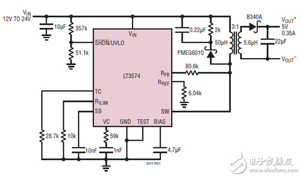
Fortunately, recent advances in power conversion technology have made low-power isolated converters much easier to design. By incorporating a primary-side sensing scheme and running the converter in boundary mode, Linear Technology’s no-opto flyback converters, such as the LT3574 and LT8300, simplify the design of flyback converters by eliminating the need for an opto-coupler, external MOSFET, secondary-side reference voltage, and extra transformer winding. Its boundary mode, which is a variable-frequency, current-mode, control switching scheme (more on this shortly), also results in improved regulation over the full line, load, and temperature ranges. According to Linear, boundary mode also permits the use of a smaller transformer compared to equivalent continuous conduction mode (CCM) designs. These flyback solutions are popular in isolated power supplies ranging from less than a watt to tens of watts.
声明:本文内容及配图由入驻作者撰写或者入驻合作网站授权转载。文章观点仅代表作者本人,不代表电子发烧友网立场。文章及其配图仅供工程师学习之用,如有内容侵权或者其他违规问题,请联系本站处理。 举报投诉
- 相关下载
- 相关文章


