
资料下载


高输入电压下变频器的高频切换
分享资料个
高输入电压下变频器的高频切换
In an effort to reduce the size of the output capacitor and inductor to save printed-circuit board (PCB) space, more and more high-input-voltageDC/DC converters are being operated at higher switching frequencies. However, as the output voltage drops to 5 V and lower, designing faster switching high-input-voltage step-down DC/DC converters is becoming difficult for several reasons. Key among them is lower duty cycle.
因此,频率超过1 MHz的转换器对电源系统的影响不仅仅局限于它的尺寸和效率。因此,在设计高输入电压和低输出电压的高开关频率的DC/DC转换器时,存在着权衡取舍。本文探讨了一些设计实例,证明了在高频率下切换高输入电压降压型DC/DC转换器的优点和缺点。
为了解释这些权衡,德克萨斯仪器工程师们建造了三个独立的电源,分别在开关频率为100, 300和750千赫时运行。在设计高频应用笔记”描述的挑战,高输入电压的直流/直流转换器”,¹所有三直流/直流转换器设计的输入电压为48 V,而输出电压为5 V 1 A根据设计者的一个输出电流,这样的降压转换器通常用于供电5 V逻辑USB或作为中间总线转换器来驱动负载点(POL)在电路板上稳压器。
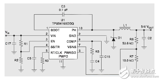
Before building the supplies, the engineers established a few design constraints. For instance, the acceptable ripple voltage was set to 1 percent of the output voltage, which in this case amounted to 50 mV. In addition, peak-to-peak inductor current selected was 0.5 A. Each design, which was based on the circuit in Figure 1, incorporates TI’s TPS54160, a 2.5 MHz, 60 V, 1.5 A step-down DC/DC converter with an integrated MOSFET.
声明:本文内容及配图由入驻作者撰写或者入驻合作网站授权转载。文章观点仅代表作者本人,不代表电子发烧友网立场。文章及其配图仅供工程师学习之用,如有内容侵权或者其他违规问题,请联系本站处理。 举报投诉
- 相关下载
- 相关文章


