资料下载

ad9861混合信号前端(MxFE™)宽带应用基带收发器数据表
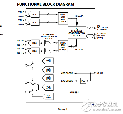
The AD9861 is a member of the MxFE family—a group of integrated converters for the communications market. The AD9861 integrates dual 10-bit analog-to-digital converters (ADC) and dual 10-bit digital-to-analog converters (TxDAC®)。 Two speed grades are available, -50 and -80. The -50 is optimized for ADC sampling of 50 MSPS and less, while the -80 is optimized for ADC sample rates between 50 MSPS and 80 MSPS. The dual TxDACs operate at speeds up to 200 MHz and include a bypassable 2× or 4× interpolation filter. Three auxiliary converters are also available to provide required system level control voltages or to monitor system signals. The AD9861 is optimized for high performance, low power, small form factor, and to provide a cost-effective solution for the broadband communication market. The AD9861 uses a single input clock pin (CLKIN) to generate all system clocks. The ADC and TxDAC clocks are generated within a timing generation block that provides user programmable options such as divide circuits, PLL multipliers, and switches. A flexible, bidirectional 20-bit I/O bus accommodates a variety of custom digital back ends or open market DSPs. In half-duplex systems, the interface supports 20-bit parallel transfers or 10-bit interleaved transfers. In full-duplex systems, the interface supports an interleaved 10-bit ADC bus and an interleaved 10-bit TxDAC bus. The flexible I/O bus reduces pin count and, therefore, reduces the required package size on the AD9861 and the device to which it connects. The AD9861 can use either mode pins or a serial programmable interface (SPI) to configure the interface bus, operate the ADC in a low power mode, configure the TxDAC interpolation rate, and control ADC and TxDAC power-down. The SPI provides more programmable options for both the TxDAC path (for example, coarse and fine gain control and offset control for channel matching) and the ADC path (for example, the internal duty cycle stabilizer, and twos complement data format)。 The AD9861 is packaged in a 64-lead LFCSP (low profile, fine pitched, chip scale package)。 The 64-lead LFCSP footprint is only 9 mm × 9 mm, and is less than 0.9 mm high, fitting into tightly spaced applications such as PCMCIA cards.

声明:本文内容及配图由入驻作者撰写或者入驻合作网站授权转载。文章观点仅代表作者本人,不代表电子发烧友网立场。文章及其配图仅供工程师学习之用,如有内容侵权或者其他违规问题,请联系本站处理。 举报投诉
- 相关下载
- 相关文章


