
资料下载


LC2 MOS信号调理ADC的RTD励磁电流AD7711
分享资料个
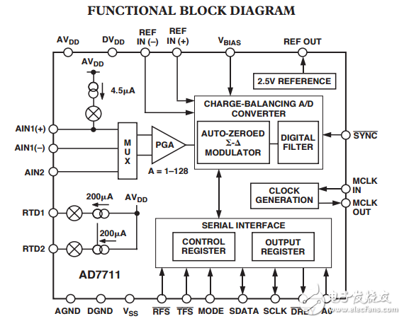
The AD7711 is a complete analog front end for low frequency measurement applications. The device accepts low level signals directly from a transducer and outputs a serial digital word. It employs a :- conversion technique to realize up to 24 bits of no missing codes performance. The input signal is applied to a proprietary programmable gain front end based around an analog modulator. The modulator output is processed by an on-chip digital filter. The first notch of this digital filter can be programmed via the on-chip control register, allowing adjustment of the filter cutoff and settling time. The part features one differential analog input and one singleended analog input as well as a differential reference input. Normally, one of the input channels will be used as the main channel with the second channel used as an auxiliary input to periodically measure a second voltage. It can be operated from a single supply (by tying the VSS pin to AGND), provided that the input signals on the analog inputs are more positive than –30 mV. By taking the VSS pin negative, the part can convert signals down to –VREF on its inputs. The part provides two current sources that can be used to provide excitation in 3-wire and 4-wire RTD configurations. The AD7711 thus performs all signal conditioning and conversion for a single- or dual-channel system. AD7711 The AD7711 is ideal for use in smart, microcontroller based systems. Gain settings, signal polarity, input channel selection, and RTD current control can be configured in software using the bidirectional serial port. The AD7711 contains selfcalibration, system calibration, and background calibration options, and also allows the user to read and write the on-chip calibration registers. CMOS construction ensures low power dissipation, and a software programmable power-down mode reduces the standby power consumption to only 7 mW typical. The part is available in a 24-lead, 0.3-inch-wide, plastic and hermetic dual-in-line package (DIP) as well as a 24-lead small outline (SOIC) package.
声明:本文内容及配图由入驻作者撰写或者入驻合作网站授权转载。文章观点仅代表作者本人,不代表电子发烧友网立场。文章及其配图仅供工程师学习之用,如有内容侵权或者其他违规问题,请联系本站处理。 举报投诉
- 相关下载
- 相关文章


