
资料下载


基于TQC9312下的3.3 – 3.8 GHz ½ W Digital Variable Gain Amplifier
张生
分享资料个
Applications
3G / 4G Wireless Infrastructure
Repeaters Small cells
General Description
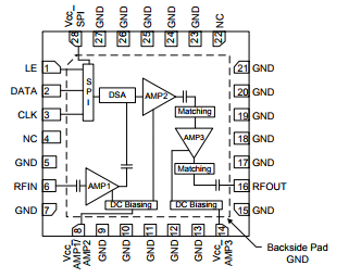
The TQC9312 is a digital variable gain amplifier (DVGA) featuring high linearity over the entire gain control range. This amplifier module integrates two gain blocks, a digital-step attenuator (DSA), and a high linearity ½ W amplifier.
The module has the added feature of integrating all matching components, bias chokes and blocking capacitors. The internal 6-bit DSA provides a 31.5 dB gain control range in 0.5 dB steps, and is controlled with a serial periphery interface (SPITM)。 The TQC9312 features variable gain from 9 dB to 40dB at 3.5 GHz, +44.5 dBm output IP3, and +27.8 dBm P1dB. The module operates from a single +5V supply and is available in a compact 28-pin 6x6 mm leadless SMT package.
The TQC9312 is pin compatible with the TQM879008 (1.5-2.7GHz, 0.5W P1dB) and TQM879006A (1.4- 2.7GHz, 0.25W P1dB)。 This allows one to size the right type of device for specific system level requirements as well as making the DVGA family ideal for applications where a common PCB layout is used for different frequency bands.

声明:本文内容及配图由入驻作者撰写或者入驻合作网站授权转载。文章观点仅代表作者本人,不代表电子发烧友网立场。文章及其配图仅供工程师学习之用,如有内容侵权或者其他违规问题,请联系本站处理。 举报投诉
- 相关下载
- 相关文章


