资料下载

MC74HC367_datasheet
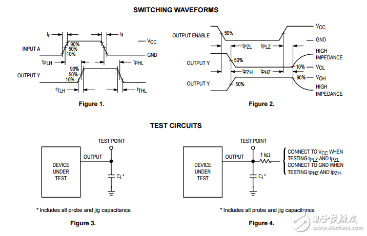
The MC54/74HC367 is identical in pinout to the LS367. The device inputs are compatible with standard CMOS outputs; with pullup resistors, they are compatible with LSTTL outputs. This device is arranged into 2–bit and 4–bit sections, each having its own active–low Output Enable. When either of the enables is high, the affected buffer outputs are placed into high–impedance states. The HC367 has noninverting outputs. • Output Drive Capability: 15 LSTTL Loads • Outputs Directly Interface to CMOS, NMOS, and TTL • Operating Voltage Range: 2 to 6 V • Low Input Current: 1 µA • High Noise Immunity Characteristic of CMOS Devices • In Compliance with the Requirements Defined by JEDEC Standard No. 7A • Chip Complexity: 92 FETs or 23 Equivalent Gates

声明:本文内容及配图由入驻作者撰写或者入驻合作网站授权转载。文章观点仅代表作者本人,不代表电子发烧友网立场。文章及其配图仅供工程师学习之用,如有内容侵权或者其他违规问题,请联系本站处理。 举报投诉
- 相关下载
- 相关文章


