
资料下载


一个更好的方式在LED背光管理漏电流故障

分享资料个
一个更好的方式在LED背光管理漏电流故障
一个标准的方式来配置一个背光是使用两个分立器件:100 V MOSFET在DPAK封装和100 V肖特基二极管,也在采用DPAK封装。肖特基二极管的高漏电流可能是在LED背光单元,特别是在较高的温度下的问题。一些客户在大规模生产过程中经历了肖特基二极管的泄漏故障问题。提高泄漏故障的一种方法是增加肖特基二极管的电压等级从100 V至120 V,但泄漏电流仍然可以是一个问题时,系统温度高。
我们的设计团队开发了一种替代的方法,利用飞兆半导体的新的100 V boostpak溶液。BoostPak家族(图1)使用一个单一的包家两设备:100 V和150 V NP二极管的MOSFET。
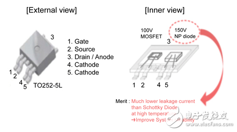
Figure 1: The BoostPak combines a 100 V MOSFET and a 150 V NP diode into one package.
The BoostPak family is housed in a single 5-lead DPAK package. The N-channel MOSFET has been tailored to minimize the on-state resistance while maintaining superior switching performance. The NP diode is a hyperfast rectifier with low forward voltage drop and excellent switching performance. It has a much lower leakage current than a Schottky diode, so it delivers better system reliability in high-temperature applications.
Compared to the two-discrete solution, the BoostPak approach uses a smaller footprint and can save as much as 20 mm² of PCB space. Using one package instead of two also means there is less assembly work and lower system cost.
声明:本文内容及配图由入驻作者撰写或者入驻合作网站授权转载。文章观点仅代表作者本人,不代表电子发烧友网立场。文章及其配图仅供工程师学习之用,如有内容侵权或者其他违规问题,请联系本站处理。 举报投诉
- 相关下载
- 相关文章




