资料下载

Microchip的mrf49xaISM频段射频收发器数据表
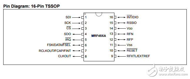
Microchip’s MRF49XA is a fully integrated Sub-GHz RF transceiver. This low-power single chip Frequency Shift Keying (FSK) baseband transceiver supports: • Zero-IF architecture • Multi-channel and multi-band • Synthesizer with PLL • Power Amplifier (PA) • Low Noise Amplifier (LNA) • I/Q down converter mixers • I/Q demodulator • Baseband filters (BBFs) and amplifiers The simplified functional block diagram of MRF49XA is shown in Figure 1-1. The MRF49XA is an ideal choice for low-cost, high-volume, low data rate (《256 kbps), two-way and short range wireless applications. This transceiver can be used in the unlicensed 433 MHz, 868 MHz and 915 MHz frequency bands, and for applications looking for FCC, IC or ETSI certification in the ISM band. The MRF49XA has a low phase noise and provides an excellent adjacent channel interference, Bit Error Rate (BER) and larger communication coverage along with higher output power.
The MRF49XA device’s AFC feature allows for the use of a low-accuracy, low-cost crystal. In order to minimize the total system cost, a communication link in most of the applications can be created using a low-cost, generic 10 MHz crystal, a bypass filter and an affordable microcontroller. The MRF49XA provides a clock signal for the microcontroller and avoids the need for a second crystal on the circuit board. The transceiver can be interfaced with many popular Microchip PIC® microcontrollers through a 4-wire SPI, interrupt (IRO) and Reset. The interface between the microcontroller and MRF49XA is shown in Figure 1-2. The MRF49XA supports the following digital data processing features: • PLL and I/Q VCO with Calibration • Receiver Signal Strength Indicator • Data Quality Indicator • AFC • Baseband Power Amplifier • TX and RX Buffers The receiver’s Baseband Bandwidth (BBBW) can be programmed to accommodate various deviations, data rates and crystal tolerance requirements. The high-resolution PLL allows: • The usage of multiple channels in any of the bands • The rapid settling time allows for faster frequency hopping, bypassing multipath fading and interference to achieve robust wireless links The transceiver is integrated with different Sleep modes and an internal wake-up timer to reduce the overall current consumption, and to extend the battery life. The device’s small size with low-power consumption makes it ideal for various short range radio applications.

声明:本文内容及配图由入驻作者撰写或者入驻合作网站授权转载。文章观点仅代表作者本人,不代表电子发烧友网立场。文章及其配图仅供工程师学习之用,如有内容侵权或者其他违规问题,请联系本站处理。 举报投诉
- 相关下载
- 相关文章


