
资料下载


LC2 MOS四路14位数模转换器AD7834/AD7835数据表
分享资料个
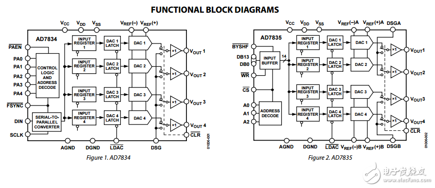
The AD7834 and AD7835 contain four 14-bit DACs on one monolithic chip. The AD7834 and AD7835 have output voltages in the range ±8.192 V with a maximum span of 14 V. The AD7834 is a serial input device. Data is loaded in 16-bit format from the external serial bus, MSB first after two leading 0s, into one via DIN, SCLK, and FSYNC. The AD7834 has five dedicated package address pins, PA0 to PA4, that can be wired to AGND or VCC to permit up to 32 AD7834s to be individually addressed in a multipackage application. The AD7835 can accept either 14-bit parallel loading or doublebyte loading, where right-justified data is loaded in one 8-bit byte and one 6-bit byte. Data is loaded from the external bus into one of the input latches under the control of the WR, CS, BYSHF, and DAC channel address pins, A0 to A2. With each device, the LDAC signal is used to update all four DAC outputs simultaneously, or individually, on reception of new data. In addition, for each device, the asynchronous CLR input can be used to set all signal outputs, VOUT1 to VOUT4, to the user-defined voltage level on the device sense ground pin, DSG. On power-on, before the power supplies have stabilized, internal circuitry holds the DAC output voltage levels to within ±2 V of the DSG potential. As the supplies stabilize, the DAC output levels move to the exact DSG potential (assuming CLR is exercised)。 The AD7834 is available in a 28-lead 0.3“ SOIC package and a 28-lead 0.6” PDIP package, and the AD7835 is available in a 44-lead MQFP package and a 44-lead PLCC package.
声明:本文内容及配图由入驻作者撰写或者入驻合作网站授权转载。文章观点仅代表作者本人,不代表电子发烧友网立场。文章及其配图仅供工程师学习之用,如有内容侵权或者其他违规问题,请联系本站处理。 举报投诉
- 相关下载
- 相关文章


