资料下载

2.3v最小SPI串行闪存AT45DB321E
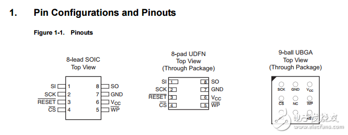
The Adesto® AT45DB321E is a 2.3V minimum, serial-interface sequential access Flash memory ideally suited for a wide variety of digital voice, image, program code, and data storage applications. The AT45DB321E also supports the RapidS serial interface for applications requiring very high speed operation. Its 34,603,008 bits of memory are organized as 8,192 pages of 512 bytes or 528 bytes each. In addition to the main memory, the AT45DB321E also contains two SRAM buffers of 512/528 bytes each. The buffers allow receiving of data while a page in the main memory is being reprogrammed. Interleaving between both buffers can dramatically increase a system‘s ability to write a continuous data stream. In addition, the SRAM buffers can be used as additional system scratch pad memory, and E2 PROM emulation (bit or byte alterability) can be easily handled with a self-contained three step read-modify-write operation. Unlike conventional Flash memories that are accessed randomly with multiple address lines and a parallel interface, the Adesto DataFlash® uses a serial interface to sequentially access its data. The simple sequential access dramatically reduces active pin count, facilitates simplified hardware layout, increases system reliability, minimizes switching noise, and reduces package size. The device is optimized for use in many commercial and industrial applications where high-density, low-pin count, low-voltage, and low-power are essential. To allow for simple in-system re-programmability, the AT45DB321E does not require high input voltages for programming. The device operates from a single 2.3V to 3.6V power supply for the erase and program and read operations. The AT45DB321E is enabled through the Chip Select pin (CS) and accessed via a 3-wire interface consisting of the Serial Input (SI), Serial Output (SO), and the Serial Clock (SCK)。 All programming and erase cycles are self-timed.

声明:本文内容及配图由入驻作者撰写或者入驻合作网站授权转载。文章观点仅代表作者本人,不代表电子发烧友网立场。文章及其配图仅供工程师学习之用,如有内容侵权或者其他违规问题,请联系本站处理。 举报投诉
- 相关下载
- 相关文章


