
资料下载


×
72兆位QDR®II SRAM两词突发结构CY7C1512KV18-300BZXC
消耗积分:0 |
格式:rar |
大小:0.92 MB |
2017-09-14
分享资料个
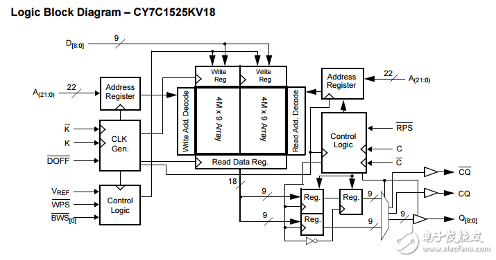
The CY7C1525KV18, CY7C1512KV18, and CY7C1514KV18 are 1.8 V synchronous pipelined SRAMs, equipped with QDR II architecture. QDR II architecture consists of two separate ports: the read port and the write port to access the memory array. The read port has dedicated data outputs to support read operations and the write port has dedicated data inputs to support write operations. QDR II architecture has separate data inputs and data outputs to completely eliminate the need to “turnaround” the data bus that exists with common I/O devices. Access to each port is through a common address bus. Addresses for read and write addresses are latched on alternate rising edges of the input (K) clock. Accesses to the QDR II read and write ports are completely independent of one another. To maximize data throughput, both read and write ports are equipped with DDR interfaces. Each address location is associated with 9-bit words (CY7C1525KV18), 18-bit words (CY7C1512KV18), or 36-bit words (CY7C1514KV18) that burst sequentially into or out of the device. Because data can be transferred into and out of the device on every rising edge of both input clocks (K and K and C and C), memory bandwidth is maximized while simplifying system design by eliminating bus turnarounds. Depth expansion is accomplished with port selects, which enables each port to operate independently. All synchronous inputs pass through input registers controlled by the K or K input clocks. All data outputs pass through output registers controlled by the C or C (or K or K in a single clock domain) input clocks. Writes are conducted with on-chip synchronous self-timed write circuitry. For a complete list of related documentation, click here.
声明:本文内容及配图由入驻作者撰写或者入驻合作网站授权转载。文章观点仅代表作者本人,不代表电子发烧友网立场。文章及其配图仅供工程师学习之用,如有内容侵权或者其他违规问题,请联系本站处理。 举报投诉
评论(0)
发评论
- 相关下载
- 相关文章


