
资料下载


3.3 V CMOS SRAM 64K×16,AS7C31026B数据手册
分享资料个
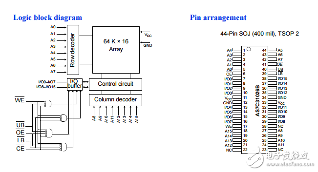
The AS7C31026B is a high-performance CMOS 1,048,576-bit Static Random Access Memory (SRAM) device organized as 65,536 words × 16 bits. It is designed for memory applications where fast data access, low power, and simple interfacing are desired. Equal address access and cycle times (tAA, tRC, tWC) of 10/12/15/20 ns with output enable access times (tOE) of 5, 6, 7, 8 ns are ideal for high-performance applications. When CE is high, the device enters standby mode. A write cycle is accomplished by asserting write enable (WE) and chip enable (CE)。 Data on the input pins I/O0 through I/O15 is written on the rising edge of WE (write cycle 1) or CE (write cycle 2)。 To avoid bus contention, external devices should drive I/O pins only after outputs have been disabled with output enable (OE) or write enable (WE)。 A read cycle is accomplished by asserting output enable (OE) and chip enable (CE) with write enable (WE) high. The chips drive I/O pins with the data word referenced by the input address. When either chip enable or output enable is inactive or write enable is active, output drivers stay in high-impedance mode. The device provides multiple center power and ground pins, and separate byte enable controls, allowing individual bytes to be written and read. LB controls the lower bits, I/O0 through I/O7, and UB controls the higher bits, I/O8 through I/O15. All chip inputs and outputs are TTL-compatible, and operation is from a single 3.3 V supply. The device is packaged in common industry standard packages.
声明:本文内容及配图由入驻作者撰写或者入驻合作网站授权转载。文章观点仅代表作者本人,不代表电子发烧友网立场。文章及其配图仅供工程师学习之用,如有内容侵权或者其他违规问题,请联系本站处理。 举报投诉
- 相关下载
- 相关文章


