
资料下载


DDR2_DDR3_SDRAM,PCB布线规则指导
分享资料个
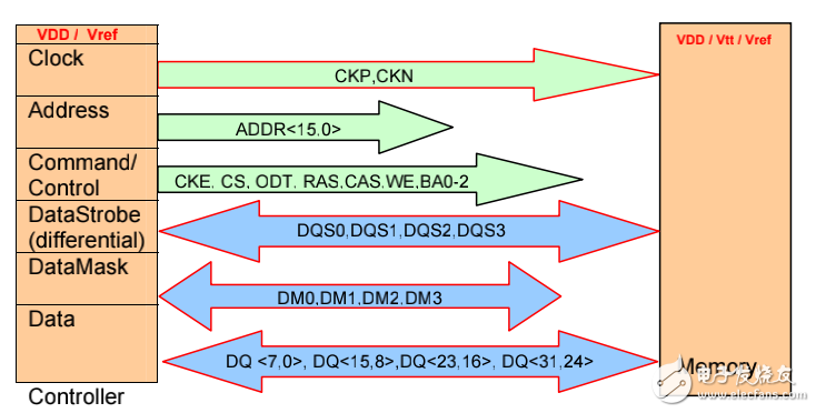
DDR2 usage is common today with a push towards higher speeds such as 800 Mbps [1] and more recently,
1066 Mbps. DDR3 [2] targets a data rate of 1600 Mbps. From a PCB implementation standpoint, a primary
requirement is delay matching which is dictated by the timing requirement. This brings into it a number of related
factors that affect waveform integrity and delay. These factors are interdependent, but where a distinction can
be made, they can be termed PCB layer stackup and impedance, interconnect topologies, delay matching, cross
talk, PI and timing. Cadence ALLEGRO™SI-230 and Ansoft’s HFSS™ are used in all computations.
声明:本文内容及配图由入驻作者撰写或者入驻合作网站授权转载。文章观点仅代表作者本人,不代表电子发烧友网立场。文章及其配图仅供工程师学习之用,如有内容侵权或者其他违规问题,请联系本站处理。 举报投诉
- 相关下载
- 相关文章


