
资料下载


cy7c1353g 4兆位(256K SRAM×18)流过诺博™架构
分享资料个
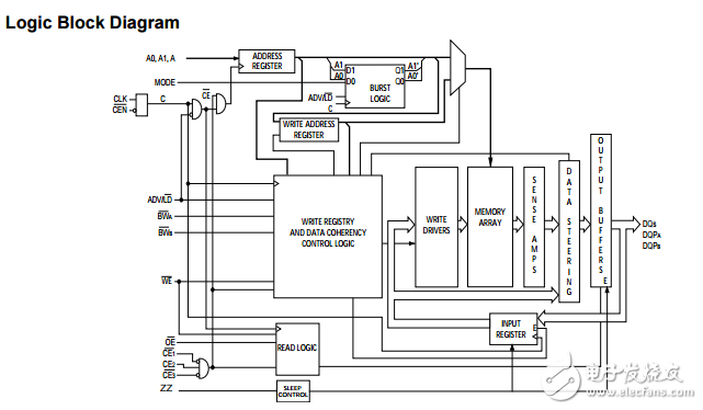
he CY7C1353G is a 3.3 V, 256K × 18 synchronous flow-through burst SRAM designed specifically to support unlimited true back-to-back read/write operations without the insertion of wait states. The CY7C1353G is equipped with the advanced No Bus Latency™ (NoBL™) logic required to enable consecutive read/write operations with data being transferred on every clock cycle. This feature dramatically improves the throughput of data through the SRAM, especially in systems that require frequent write-read transitions. All synchronous inputs pass through input registers controlled by the rising edge of the clock. The clock input is qualified by the clock enable (CEN) signal, which when deasserted suspends operation and extends the previous clock cycle. Maximum access delay from the clock rise is 8.0 ns (100-MHz device)。 Write operations are controlled by the two byte write select (BW[A:B]) and a write enable (WE) input. All writes are conducted with on-chip synchronous self timed write circuitry. Three synchronous chip enables (CE1, CE2, CE3) and an asynchronous output enable (OE) provide for easy bank selection and output tri-state control. To avoid bus contention, the output drivers are synchronously tri-stated during the data portion of a write sequence. For a complete list of related documentation, click here.
声明:本文内容及配图由入驻作者撰写或者入驻合作网站授权转载。文章观点仅代表作者本人,不代表电子发烧友网立场。文章及其配图仅供工程师学习之用,如有内容侵权或者其他违规问题,请联系本站处理。 举报投诉
- 相关下载
- 相关文章


