
资料下载


cy7c1347g 4兆位(128K的×36)流水线同步SRAM
分享资料个
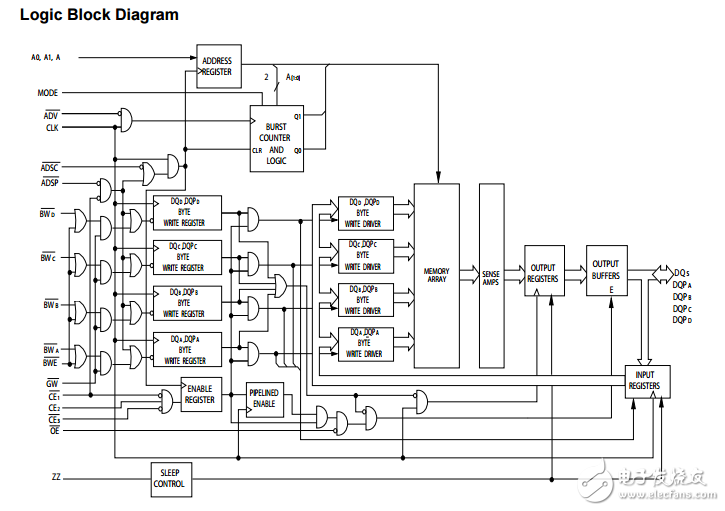
The CY7C1347G is a 3.3 V, 128K × 36 synchronous pipelined SRAM designed to support zero-wait-state secondary cache with minimal glue logic. CY7C1347G I/O pins can operate at either the 2.5 V or the 3.3 V level. The I/O pins are 3.3 V tolerant when VDDQ = 2.5 V. All synchronous inputs pass through input registers controlled by the rising edge of the clock. All data outputs pass through output registers controlled by the rising edge of the clock. Maximum access delay from the clock rise is 2.6 ns (250 MHz device)。 CY7C1347G supports either the interleaved burst sequence used by the Intel Pentium processor or a linear burst sequence used by processors such as the PowerPC. The burst sequence is selected through the MODE pin. Accesses can be initiated by asserting either the address strobe from processor (ADSP) or the address strobe from controller (ADSC) at clock rise. Address advancement through the burst sequence is controlled by the ADV input. A 2-bit on-chip wraparound burst counter captures the first address in a burst sequence and automatically increments the address for the rest of the burst access. Byte write operations are qualified with the four Byte Write Select (BW[A:D]) inputs. A global write enable (GW) overrides all byte write inputs and writes data to all four bytes. All writes are conducted with on-chip synchronous self timed write circuitry. Three synchronous chip Selects (CE1, CE2, CE3) and an asynchronous output enable (OE) provide for easy bank selection and output tristate control. To provide proper data during depth expansion, OE is masked during the first clock of a read cycle when emerging from a deselected state. For a complete list of related documentation, click here.
声明:本文内容及配图由入驻作者撰写或者入驻合作网站授权转载。文章观点仅代表作者本人,不代表电子发烧友网立场。文章及其配图仅供工程师学习之用,如有内容侵权或者其他违规问题,请联系本站处理。 举报投诉
- 相关下载
- 相关文章


