
资料下载


9-mbit流过的SRAMCY7C1361C/CY7C1363C
分享资料个
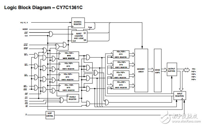
Functional Description The CY7C1361C/CY7C1363C is a 3.3 V, 256K × 36/512K × 18 synchronous flow-through SRAMs, respectively designed to interface with high speed microprocessors with minimum glue logic. Maximum access delay from clock rise is 6.5 ns (133 MHz version)。 A 2-bit on-chip counter captures the first address in a burst and increments the address automatically for the rest of the burst access. All synchronous inputs are gated by registers controlled by a positive-edge-triggered clock input (CLK)。 The synchronous inputs include all addresses, all data inputs, address-pipelining chip enable (CE1), depth-expansion chip enables (CE2 and CE3 [1]), burst control inputs (ADSC, ADSP, and ADV), write enables (BWx, and BWE), and global write (GW)。 Asynchronous inputs include the output enable (OE) and the ZZ pin. The CY7C1361C/CY7C1363C enables either interleaved or linear burst sequences, selected by the MODE input pin. A HIGH selects an interleaved burst sequence, while a LOW selects a linear burst sequence. Burst accesses can be initiated with the processor address strobe (ADSP) or the cache controller address strobe (ADSC) inputs. Address advancement is controlled by the address advancement (ADV) input. Addresses and chip enables are registered at rising edge of clock when either address strobe processor (ADSP) or address strobe controller (ADSC) are active. Subsequent burst addresses can be internally generated as controlled by the advance pin (ADV)。 The CY7C1361C/CY7C1363C operates from a +3.3 V core power supply while all outputs may operate with either a +2.5 or +3.3 V supply. All inputs and outputs are JEDEC-standard JESD8-5-compatible. For a complete list of related documentation, click here
声明:本文内容及配图由入驻作者撰写或者入驻合作网站授权转载。文章观点仅代表作者本人,不代表电子发烧友网立场。文章及其配图仅供工程师学习之用,如有内容侵权或者其他违规问题,请联系本站处理。 举报投诉
- 相关下载
- 相关文章


