
资料下载


2兆位单操作电压串行闪存与100 MHz的双输出SPI总线接口IS25LD020
分享资料个
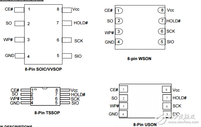
The IS25CD512/010 and IS25LD020 are 512Kbit/ 1Mbit / 2Mbit Serial Peripheral Interface (SPI) Flash memories, providing single- or dual-output. The devices are designed to support a 33 MHz clock rate in normal read mode, and 100 MHz in fast read, the fastest in the industry. The devices use a single low voltage power supply, wide operating voltage ranging to perform read, erase and program operations. The devices can be programmed in standard EPROM programmers. The IS25CD512/010 and IS25LD020 are accessed through a 4-wire SPI Interface consisting of Serial Data Input/Output (SlO), Serial Data Output (SO), Serial Clock (SCK), and Chip Enable (CE#) pins. They comply with all recognized command codes and operations. The dual-output fast read operation provides and effective serial data rate of 200MHz. The devices support page program mode, where 1 to 256 bytes data can be programmed into the memory in one program operation. These devices are divided into uniform 4 KByte sectors or uniform 32 KByte blocks.(IS25LD020 is uniform 4 KByte sectors or uniform 64 KByte)。 The IS25CD512/010 and IS25LD020 are manufactured on pFLASH™’s advanced non-volatile technology. The devices are offered in a variety of packages for all critical needs. The devices operate at wide temperatures between -40°C to +105°C.
声明:本文内容及配图由入驻作者撰写或者入驻合作网站授权转载。文章观点仅代表作者本人,不代表电子发烧友网立场。文章及其配图仅供工程师学习之用,如有内容侵权或者其他违规问题,请联系本站处理。 举报投诉
- 相关下载
- 相关文章


