
资料下载


低功耗的24位ADC与真正的轨到轨缓冲区ad7172-2数据表
分享资料个
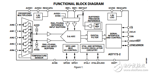
The AD7172-2 is an intelligent, low noise, low power, multiplexed, Σ-Δ analog-to-digital converter (ADC) with 2- or 4-channel (fully differential/single-ended) inputs for low bandwidth signals. The AD7172-2 has a maximum channel scan rate of 6.21 kSPS (161 µs) for fully settled data. The output data rates range from 1.25 SPS to 31.25 kSPS. The AD7172-2 integrates key analog and digital signal conditioning blocks to allow users to configure an individual setup for each analog input channel in use via the SPI. Integrated true rail-to-rail buffers on the analog inputs and external reference inputs provide easy to drive high impedance inputs. The precision 2.5 V low drift (2 ppm/°C) band gap internal reference (with an output reference buffer) adds embedded functionality to reduce the external component count. The digital filter allows simultaneous 50 Hz and 60 Hz rejection at a 27.27 SPS output data rate. The user can switch between different filter options according to the demands of each channel in the application, with further digital processing functions such as offset and gain calibration registers, which are also configurable on a per channel basis. General-purpose inputs/outputs (GPIOs) control external multiplexers synchronous to the ADC conversion timing. The specified operating temperature range is −40°C to +105°C. The AD7172-2 is in a 24-lead TSSOP package. Note that, throughout this data sheet, the dual function pin names are referenced by the relevant function only
声明:本文内容及配图由入驻作者撰写或者入驻合作网站授权转载。文章观点仅代表作者本人,不代表电子发烧友网立场。文章及其配图仅供工程师学习之用,如有内容侵权或者其他违规问题,请联系本站处理。 举报投诉
- 相关下载
- 相关文章


