
资料下载


PWM控制器处理多个拓扑结构与负输入电压
分享资料个
PWM控制器处理多个拓扑结构与负输入电压
传统上,电信和数据通信设备提供负的直流输出电压,如48伏,为系统总线。原因很简单:直流电压保持低噪音,可以容易地产生从普通铅酸电池,通常约12伏特。此外,负电源使电缆和铜线远离腐蚀。通常情况下,在应用服务器和计算机,这不受管制的负直流输出电压倒正母线电压驱动各种降压转换器,必须产生一个稳压直流低电压高电流输出驱动一个范围广泛的系统主板上的电子负载。这种系统板还使用诸如放大器,运算放大器和传感器的运作,调节,负电源或分裂的供应,以保持交流信号清洁。
将这种不受管制的负电源转换成一个受规管的负降压电源或一个调节的负升压电压,以及一个积极的调节电压,是不平凡的。每个拓扑结构是复杂和耗时的分立元件。更重要的是,它不保证性能,可以花费更多,同时占用更多的电路板空间。
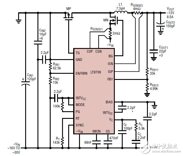
To make such a task easy for designers, Linear Technology has developed a novel synchronous multi-topology DC/DC controller, the LT8709, which can be easily configured in buck, boost, buck-boost, and inverting topologies with negative input, making it highly versatile for a wide range of power supply designs. In addition, its synchronous operation means that the output diode is replaced with a high efficiency P-channel MOSFET, thereby increasing efficiency and allowing for higher output currents up to 20 A. As a result, it eliminates the heatsink typically required in medium- to high-power applications, thus enabling a designer to generate a wide range of DC/DC conversion solutions with negative input voltage for a wide range of power supply designs.
This article investigates the architecture of this novel DC/DC controller to understand why it is so easy to generate buck, boost, and buck-boost, as well as inverting topologies with negative input voltages. Besides uncovering its unique features and functionalities, we will also present working examples of LT8709-based negative-to-negative and negative-to-positive DC/DC conversion solutions at a desired output load current. Measured performance results for a design example also will be discussed.
声明:本文内容及配图由入驻作者撰写或者入驻合作网站授权转载。文章观点仅代表作者本人,不代表电子发烧友网立场。文章及其配图仅供工程师学习之用,如有内容侵权或者其他违规问题,请联系本站处理。 举报投诉
- 相关下载
- 相关文章


