
资料下载


cy62168ev30 mobl®16兆位(2米×8)静态RAM
分享资料个
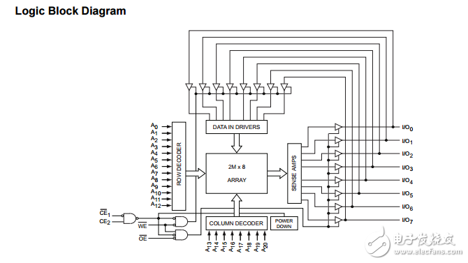
The CY62168EV30 is a high performance CMOS static RAM organized as 2 M words by 8-bits. This device features advanced circuit design to provide an ultra low active current. This is ideal for providing More Battery Life (MoBL) in portable applications such as cellular telephones. The device also has an automatic power-down feature that significantly reduces power consumption by 90% when addresses are not toggling. Placing the device into standby mode reduces power consumption by more than 99% when deselected (Chip Enable 1 (CE1) HIGH or Chip Enable 2 (CE2) LOW)。 The input and output pins (I/O0 through I/O7) are placed in a high impedance state when: the device is deselected (Chip Enable 1 (CE1) HIGH or Chip Enable 2 (CE2) LOW), outputs are disabled (OE HIGH), or a write operation is in progress (Chip Enable 1 (CE1) LOW and Chip Enable 2 (CE2) HIGH and WE LOW)。 Write to the device by taking Chip Enable 1 (CE1) LOW and Chip Enable 2 (CE2) HIGH and the Write Enable (WE) input LOW. Data on the eight I/O pins (I/O0 through I/O7) is then written into the location specified on the address pins (A0 through A20)。 Read from the device by taking Chip Enable 1 (CE1) and Output Enable (OE) LOW and Chip Enable 2 (CE2) HIGH while forcing Write Enable (WE) HIGH. Under these conditions, the contents of the memory location specified by the address pins will appear on the I/O pins. The eight input and output pins (I/O0 through I/O7) are placed in a high impedance state when the device is deselected (CE1 HIGH or CE2 LOW), the outputs are disabled (OE HIGH), or a write operation is in progress (CE1 LOW and CE2 HIGH and WE LOW)。 See the Truth Table on page 11 for a complete description of read and write modes. For a complete list of related documentation, click here.
声明:本文内容及配图由入驻作者撰写或者入驻合作网站授权转载。文章观点仅代表作者本人,不代表电子发烧友网立场。文章及其配图仅供工程师学习之用,如有内容侵权或者其他违规问题,请联系本站处理。 举报投诉
- 相关下载
- 相关文章


