
资料下载


5伏3A逻辑控制高功率开关ADP197数据表
分享资料个
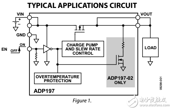
The ADP197 is a high-side load switch designed for operation between 1.8 V and 5.5 V. This load switch provides power domain isolation, which helps extend battery operation. The device contains a low on-resistance, N-channel MOSFET that supports more than 3 A of continuous current and minimizes power loss. The low 18 μA quiescent current and ultralow shutdown current make the ADP197 ideal for battery-operated portable equipment. The built-in level shifter for enable logic makes the ADP197 compatible with many processors and GPIO controllers.
Overtemperature protection circuitry activates if the junction temperature exceeds 125°C, thereby protecting itself and downstream circuits from potential damage.
The ADP197-02 incorporates an internal quick output discharge (QOD) circuit to discharge the output capacitance when the ADP197-02 output is disabled
In addition to operating performance, the ADP197 WLCSP package occupies minimal printed circuit board (PCB) space with an area of less than 1.5 mm2 and a height of 0.60 mm.
The ADP197 is available in an ultrasmall 1.0 mm × 1.5 mm, 0.5 mm pitch, 6-ball WLCSP and a 2.0 mm × 2.0 mm × 0.55 mm, 0.65 mm pitch, 6-lead LFCSP.
声明:本文内容及配图由入驻作者撰写或者入驻合作网站授权转载。文章观点仅代表作者本人,不代表电子发烧友网立场。文章及其配图仅供工程师学习之用,如有内容侵权或者其他违规问题,请联系本站处理。 举报投诉
- 相关下载
- 相关文章


