
资料下载


CMOS芯片级封装中的多路复用器ADG784数据表
分享资料个
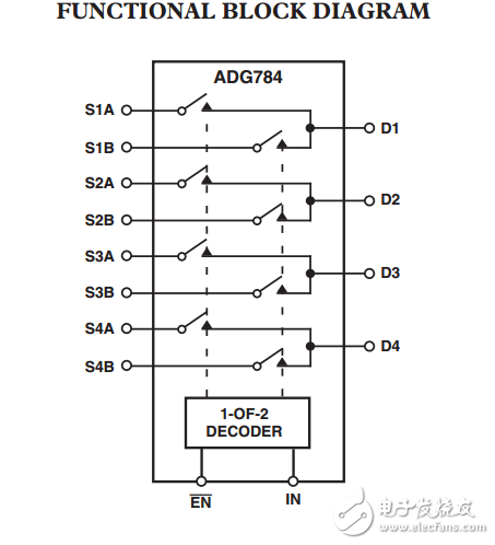
The ADG784 is a monolithic CMOS device comprising four 2:1 multiplexer/demultiplexers with high impedance outputs. The CMOS process provides low power dissipation yet gives high switching speed and low on resistance. The on-resistance variation is typically less than 0.5 Ω with an input signal ranging from 0 V to 5 V. The bandwidth of the ADG784 is greater than 200 MHz and this, coupled with low distortion (typically 0.5%), makes the part suitable for switching fast ethernet signals. The on-resistance profile is very flat over the full analog input range ensuring excellent linearity and low distortion when switching audio signals. Fast switching speed, coupled with high signal bandwidth, also makes the parts suitable for video signal switching. CMOS construction ensures ultralow power dissipation making the parts ideally suited for portable and battery powered instruments. The ADG784 operates from a single 3.3 V/5 V supply and is TTL logic compatible. The control logic for each switch is shown in the Truth Table.
These switches conduct equally well in both directions when ON, and have an input signal range that extends to the supplies. In the OFF condition, signal levels up to the supplies are blocked. The ADG784 switches exhibit break-beforemake switching action.
声明:本文内容及配图由入驻作者撰写或者入驻合作网站授权转载。文章观点仅代表作者本人,不代表电子发烧友网立场。文章及其配图仅供工程师学习之用,如有内容侵权或者其他违规问题,请联系本站处理。 举报投诉
- 相关下载
- 相关文章


