资料下载

LC2 MOS精确的5V/3V四路SPST开关ADG511/ADG512/ADG513数据表
The ADG511, ADG512 and ADG513 are monolithic CMOS ICs containing four independently selectable analog switches. These switches feature low, well-controlled on resistance and wide analog signal range, making them ideal for precision analog signal switching. These switch arrays are fabricated using Analog Devices’ advanced linear compatible CMOS (LC2 MOS) process which offers the additional benefits of low leakage currents, ultralow power dissipation and low capacitance for fast switching speeds with minimum charge injection. These features make the ADG511, ADG512 and ADG513 the optimum choice for a wide variety of signal switching tasks in precision analog signal processing and data acquisition systems. The ability to operate from single +3 V, +5 V or ±5 V bipolar supplies make the ADG511, ADG512 and ADG513 perfect for use in battery-operated instruments, 4–20 mA loop systems and with the new generation of DACs and ADCs from Analog Devices. The use of 5 V supplies and reduced operating currents give much lower power dissipation than devices operating from ±15 V supplies.
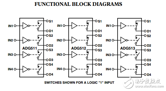
The ADG511, ADG512 and ADG513 contain four independent SPST switches. The ADG511 and ADG512 differ only in that the digital control logic is inverted. The ADG511 switch is turned on with a logic low on the appropriate control input, while a logic high is required for the ADG512. The ADG513 contains two switches whose digital control logic is similar to that of the ADG511 while the logic is inverted in the remaining two switches.

声明:本文内容及配图由入驻作者撰写或者入驻合作网站授权转载。文章观点仅代表作者本人,不代表电子发烧友网立场。文章及其配图仅供工程师学习之用,如有内容侵权或者其他违规问题,请联系本站处理。 举报投诉
- 相关下载
- 相关文章


