
资料下载


1.25MSPS的16毫瓦的内部参考和时钟12位并行模数转换器AD7492数据表
分享资料个
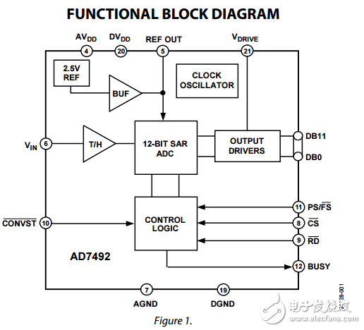
The AD7492, AD7492-4, and AD7492-5 are 12-bit high speed, low power, successive approximation ADCs. The parts operate from a single 2.7 V to 5.25 V power supply and feature throughput rates up to 1.25 MSPS. They contain a low noise, wide bandwidth track/hold amplifier that can handle bandwidths up to 10 MHz. The conversion process and data acquisition are controlled using standard control inputs allowing for easy interface to microprocessors or DSPs. The input signal is sampled on the falling edge of CONVST and conversion is also initiated at this point. The BUSY pin goes high at the start of conversion and goes low 880 ns (AD7492/AD7492-4) or 680 ns (AD7492-5) later to indicate that the conversion is complete. There are no pipeline delays associated with the part. The conversion result is accessed via standard CS and RD signals over a high speed parallel interface. The AD7492 uses advanced design techniques to achieve very low power dissipation at high throughput rates. With 5 V supplies and 1.25 MSPS, the average current consumption AD7492-5 is typically 2.75 mA. The part also offers flexible power/throughput rate management. It is also possible to operate the part in a full sleep mode and a partial sleep mode, where the part wakes up to do a conversion and automatically enters a sleep mode at the end of conversion.
声明:本文内容及配图由入驻作者撰写或者入驻合作网站授权转载。文章观点仅代表作者本人,不代表电子发烧友网立场。文章及其配图仅供工程师学习之用,如有内容侵权或者其他违规问题,请联系本站处理。 举报投诉
- 相关下载
- 相关文章


