
资料下载


完全准确的12/14/16位双VOUT nanoDAC SPI接口的4.5V至5.5V在TSSOP封装数据表ad5025/ad5045/ad5065数据表
分享资料个
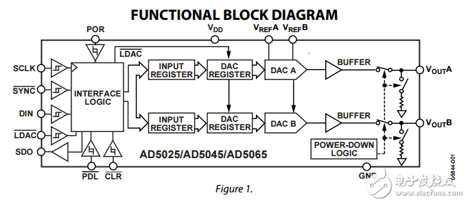
The AD5025/AD5045/AD5065 are low power, dual 12-/14-/16-bit buffered voltage output nanoDAC® DACs offering relative accuracy specifications of ±1 LSB INL with individual reference pins, and can operate from a single 4.5 V to 5.5 V supply. The AD5025/ AD5045/AD5065 also offer a differential accuracy specification of ±1 LSB. The parts use a versatile 3-wire, low power Schmitt trigger serial interface that operates at clock rates up to 50 MHz and is compatible with standard SPI®, QSPI™, MICROWIRE™, and DSP interface standards. The reference for the AD5025/ AD5045/AD5065 are supplied from an external pin and a reference buffer is provided on chip. The AD5025/AD5045/AD5065 incorporate a power-on reset circuit that ensures the DAC output powers up zero scale or midscale and remains there until a valid write takes place to the device. The AD5025/AD5045/AD5065 contain a power-down feature that reduces the current consumption of the device to typically 400 nA at 5 V and provides software selectable output loads while in power-down mode. The parts are put into power-down mode over the serial interface. Total unadjusted error for the parts is 《2.5 mV. The parts exhibit very low glitch on power-up. The outputs of all DACs can be updated simultaneously using the LDAC function, with the added functionality of user-selectable DAC channels to simultaneously update. There is also an asynchronous CLR that clears all DACs to a software-selectable code—0 V, midscale, or full scale. The parts also feature a power-down lockout pin, PDL, which can be used to prevent the DAC from entering power-down under any circumstances over the serial interface.
声明:本文内容及配图由入驻作者撰写或者入驻合作网站授权转载。文章观点仅代表作者本人,不代表电子发烧友网立场。文章及其配图仅供工程师学习之用,如有内容侵权或者其他违规问题,请联系本站处理。 举报投诉
- 相关下载
- 相关文章


