资料下载

单通道12/14/16位DAC芯片的5纳米理论参考SOT-23数据表ad5620/ad5640/AD5660
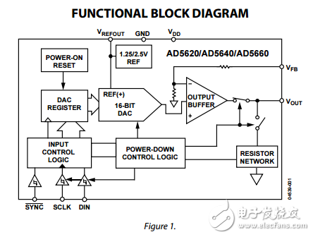
The AD5620/AD5640/AD5660, members of the nanoDAC™ family of devices, are low power, single, 12-/14-/16-bit, buffered voltage-out DACs and are guaranteed monotonic by design. The AD5620/AD5640/AD5660-1 parts include an internal, 1.25 V, 5 ppm/°C reference, giving a full-scale output voltage range of 2.5 V. The AD5620/AD5640/AD5660-2-3 parts include an internal, 2.5 V, 5 ppm/°C reference, giving a full-scale output voltage range of 5 V. The reference associated with each part is available at the VREFOUT pin. The parts incorporate a power-on reset circuit to ensure that the DAC output powers up to 0 V (AD5620/AD5640/AD5660-1-2) or midscale (AD5620-3 and AD5660-3) and remains there until a valid write takes place. The parts contain a power-down feature that reduces the current consumption of the device to 480 nA at 5 V and provides software-selectable output loads while in power-down mode. The power consumption is 2.5 mW at 5 V, reducing to 1 µW in power-down mode. The AD5620/AD5640/AD5660 on-chip precision output amplifier allows rail-to-rail output swing to be achieved. For remote sensing applications, the output amplifier’s inverting input is available to the user. The AD5620/AD5640/AD5660 use a versatile 3-wire serial interface that operates at clock rates up to 30 MHz and is compatible with standard SPI®, QSPI™, MICROWIRE™, and DSP interface standards.

声明:本文内容及配图由入驻作者撰写或者入驻合作网站授权转载。文章观点仅代表作者本人,不代表电子发烧友网立场。文章及其配图仅供工程师学习之用,如有内容侵权或者其他违规问题,请联系本站处理。 举报投诉
- 相关下载
- 相关文章


